SNVU863 july 2023
- 1
- Description
- 3
- Features
- Applications
- 6
- 1Evaluation Module Overview
- 2Hardware
- 3Implementation Results
- 4Hardware Design Files
- 5Additional Information
2.1.1.2 PWM Input
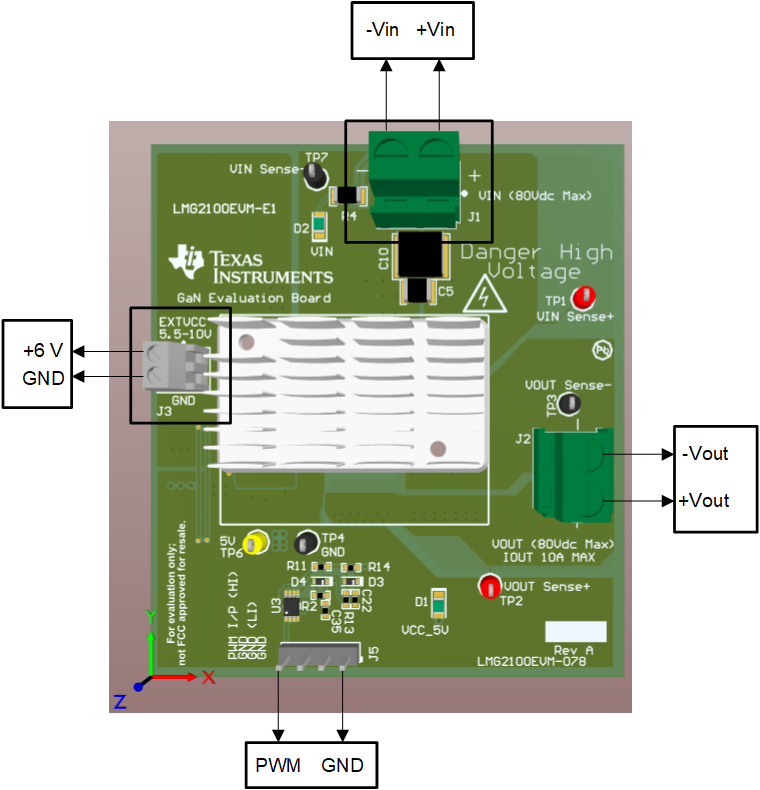
Provide the PWM input using a function generator that is capable of providing the desired switching frequency and duty cycle. This function generator output (0-5V signal) must be connected to the J5 connector as shown in the Figure 3-1. The left-most pin (pin 4) in this view is the positive input of the PWM supply and the remaining three pins are connected to GND in the default assembly for the board. The combination of R14-C22 and R2-C35 generates 8 ns to 10 ns of dead time.
Alternatively, two separate PWM inputs can be applied to control HI and LI independently. To apply this type of control, R11 must be removed, R13 must be populated with a 0-Ω resistor, and R12 must be replaced with a 10-kΩ resistor. On a board with these modifications, the HI signal must be applied at pin 4 of J5, and the LI signal at pin 2 of J5. Note that with this control scheme, the EVM no longer generates a dead time separating HI and LI transitions. Therefore, careful consideration must be applied to the control signals in this mode of operation to prevent a shoot-through condition. TI recommends to provide at least 8 ns of dead time through the external PWM signals.
 Figure 2-1 PWM Connection on J5