SPRAC94D September 2018 – March 2022 AFE030 , AFE031 , TMS320F28075 , TMS320F28075-Q1 , TMS320F28076 , TMS320F28374D , TMS320F28374S , TMS320F28375D , TMS320F28375S , TMS320F28375S-Q1 , TMS320F28376D , TMS320F28376S , TMS320F28377D , TMS320F28377D-EP , TMS320F28377D-Q1 , TMS320F28377S , TMS320F28377S-Q1 , TMS320F28379D , TMS320F28379D-Q1 , TMS320F28379S
- Trademarks
- 1 FSK Overview
- 2 Hardware Overview
- 3 Interfacing With the AFE03x
- 4 Transmit Path
- 5 Receive Path
- 6 Interfacing With a Power Line
- 7 Summary
- 8 References
- 9 Schematics
- 10Revision History
6.4.1 Metal Oxide Varistors
There are several factors to consider when selecting an MOV: Working voltage, required amount of transient energy to be absorbed by the MOV, peak transient current, and power dissipation.
 Figure 6-5 Metal Oxide Varistor (MOV)
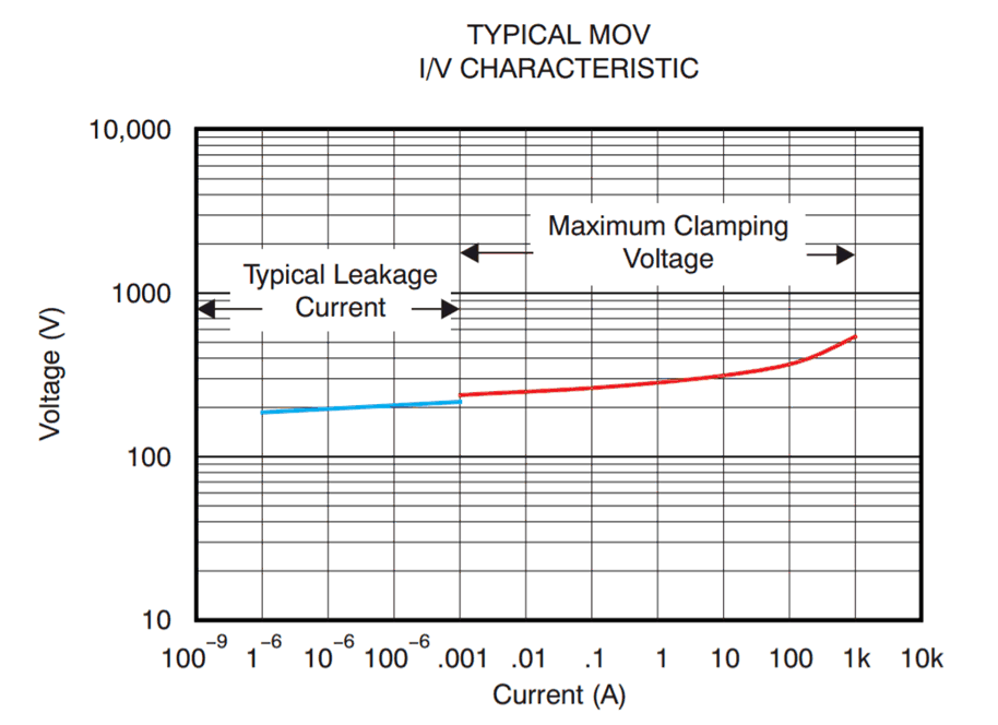
A MOV is a device that has high resistance until its triggering voltage is exceeded. Once this voltage level has been exceeded, the MOV reduces its resistance and absorbs the energy from the pulse. The I/V characteristic of a typical MOV is shown in Figure 6-6.
 Figure 6-6 Typical MOV I/V Characteristic
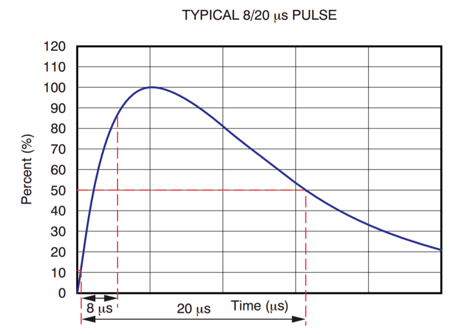
By the nature of the materials and techniques used in the construction of these components, MOVs respond quickly to a fast transient pulse, have high instantaneous power ratings, and are well-suited for protection on the ac line. The maximum clamping voltages are typically specified in response to a high-speed transient similar to that shown in Figure 6-7. The 8/20 µs waveform is commonly associated as a waveform that represents the spectral content of lightning strikes.
 Figure 6-7 Typical 8/20-µs Pulse for MOV and TVS Performance Specification