SPRADG4A January   2024  – April 2024


  1.   1
  2.   Abstract
  3.   Trademarks
  4. 1General Texas Instruments High Voltage Evaluation (TI HV EVM) User Safety Guidelines
  5. 2Introduction
  6. 3System Description
    1. 3.1 Key System Specifications
  7. 4System Overview
    1. 4.1 Block Diagram
    2. 4.2 Basic Operation
    3. 4.3 System Design Theory
      1. 4.3.1 Peak Current Mode Control (PCMC) Implementation
      2. 4.3.2 Zero Voltage Switching (ZVS) or Low Voltage Switching (LVS)
      3. 4.3.3 Synchronous Rectification
      4. 4.3.4 Slope Compensation
  8. 5Hardware
    1. 5.1 Hardware Overview
    2. 5.2 Hardware and Test Instruments Required
    3. 5.3 TMDSCNCD263 controlCARD™ Changes
  9. 6Software
    1. 6.1 Getting Started With Firmware
      1. 6.1.1 Opening the Code Composer Studio Project
      2. 6.1.2 Software Architecture
      3. 6.1.3 Project Folder Structure
    2. 6.2 SysConfig Setup
      1. 6.2.1 EPWM Configuration
      2. 6.2.2 ADC Configuration
      3. 6.2.3 CMPSS Configuration
    3. 6.3 Incremental Builds
      1. 6.3.1 Procedure for Running the Incremental Builds - PCMC
        1. 6.3.1.1 Lab 1: Phase Overlapping Check With Open Current and Voltage Loop
          1. 6.3.1.1.1 Objective of Lab 1
          2. 6.3.1.1.2 Overview of Lab 1
          3. 6.3.1.1.3 Procedure of Lab 1
            1. 6.3.1.1.3.1 Start CCS and Open a Project for Lab 1
            2. 6.3.1.1.3.2 Build and Load the Project for Lab 1
            3. 6.3.1.1.3.3 Debug Environment Windows for Lab 1
            4. 6.3.1.1.3.4 Run the Code for Lab 1
        2. 6.3.1.2 Lab 2: Closed Current and Open Voltage Loop
          1. 6.3.1.2.1 Objective of Lab 2
          2. 6.3.1.2.2 Overview of Lab 2
          3. 6.3.1.2.3 Procedure of Lab 2
            1. 6.3.1.2.3.1 Build and Load Project for Lab 2
            2. 6.3.1.2.3.2 Debug Environment Windows for Lab 2
            3. 6.3.1.2.3.3 Run the Code for Lab 2
        3. 6.3.1.3 Lab 3: Closed Current and Closed Voltage Loop
          1. 6.3.1.3.1 Objective of Lab 3
          2. 6.3.1.3.2 Overview of Lab 3
          3. 6.3.1.3.3 Procedure of Lab 3
            1. 6.3.1.3.3.1 Build and Load Project for Lab 3
            2. 6.3.1.3.3.2 Debug Environment Windows for Lab 3
            3. 6.3.1.3.3.3 Run the Code for Lab 3
  10. 7Testing and Results
    1. 7.1 Lab 0: Basic PWM Check
    2. 7.2 Lab 1: Phase Overlapping Check With Open Current and Voltage Loop
    3. 7.3 Lab 2: Closed Current and Open Voltage Loop
    4. 7.4 Lab 3: Closed Current and Closed Voltage Loop
  11. 8References
  12. 9Revision History

ADC Configuration

Four ADC instances have been used in this demonstration to sense all voltages, currents on the HV and LV dc bus side. PSFB_HVBUS_ADC_MODULE, PSFB_LVBUS_ADC_MODULE, PSFB_IHV_FILT_ADC_MODULE, PSFB_ILV_ADC_MODULE are assigned to the signals mentioned in Key Signal Connections. Rest of the required ADC related configurations are done in PSFB_HAL_setupADC() and PSFB_HAL_setupADCSoC() inside main().

The ADC HSEC Board Pin out is different for E1 and E2 versions of the AM263x controlCARD, which is mentioned in Table 6-1.

Table 6-1 ADC Mapping for E1 and E2 controlCARD With HSEC Board
HSEC Board E1 E2
12 ADC0_AIN0 ADC1_AIN0
14 ADC0_AIN1 ADC1_AIN1
15 ADC0_AIN2 ADC0_AIN2
18 ADC1_AIN0 ADC1_AIN2
20 ADC1_AIN1 ADC1_AIN3
21 ADC1_AIN2 ADC0_AIN4
23 ADC1_AIN3 ADC0_AIN5
28 ADC2_AIN2 ADC3_AIN0
30 ADC2_AIN3 ADC3_AIN1
31 ADC3_AIN0 ADC2_AIN0
33 ADC3_AIN1 ADC2_AIN1
34 ADC3_AIN2 ADC3_AIN2
37 ADC4_AIN0 ADC2_AIN2
39 ADC4_AIN3 ADC2_AIN3

Set the ADC DAC reference voltage switches according to application requirements by checking in the respective board schematics document in the section - ADC and DAC Interfaces.
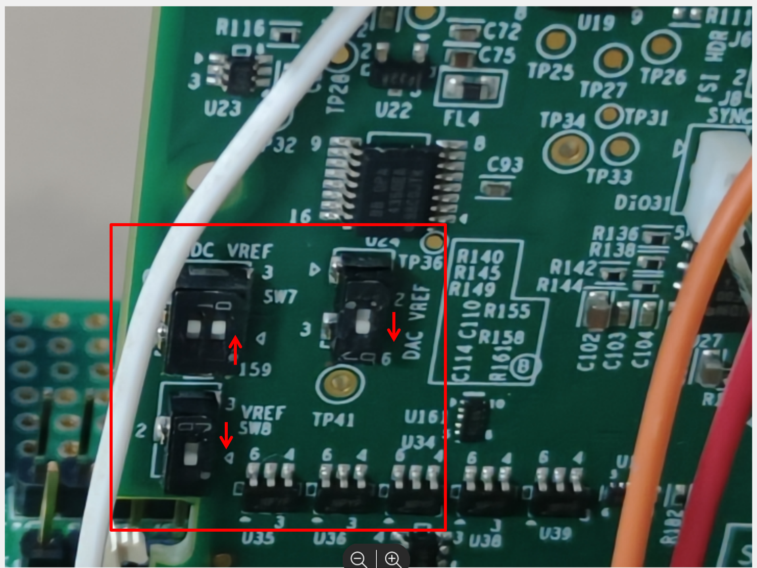
GUID-20230406-SS0I-9FVZ-V5FD-L6QGCPL0598L-low.png Figure 6-4 ADC and DAC Reference Switches in the AM263x controlCARD