SPRADG4A January   2024  – April 2024


  1.   1
  2.   Abstract
  3.   Trademarks
  4. 1General Texas Instruments High Voltage Evaluation (TI HV EVM) User Safety Guidelines
  5. 2Introduction
  6. 3System Description
    1. 3.1 Key System Specifications
  7. 4System Overview
    1. 4.1 Block Diagram
    2. 4.2 Basic Operation
    3. 4.3 System Design Theory
      1. 4.3.1 Peak Current Mode Control (PCMC) Implementation
      2. 4.3.2 Zero Voltage Switching (ZVS) or Low Voltage Switching (LVS)
      3. 4.3.3 Synchronous Rectification
      4. 4.3.4 Slope Compensation
  8. 5Hardware
    1. 5.1 Hardware Overview
    2. 5.2 Hardware and Test Instruments Required
    3. 5.3 TMDSCNCD263 controlCARD™ Changes
  9. 6Software
    1. 6.1 Getting Started With Firmware
      1. 6.1.1 Opening the Code Composer Studio Project
      2. 6.1.2 Software Architecture
      3. 6.1.3 Project Folder Structure
    2. 6.2 SysConfig Setup
      1. 6.2.1 EPWM Configuration
      2. 6.2.2 ADC Configuration
      3. 6.2.3 CMPSS Configuration
    3. 6.3 Incremental Builds
      1. 6.3.1 Procedure for Running the Incremental Builds - PCMC
        1. 6.3.1.1 Lab 1: Phase Overlapping Check With Open Current and Voltage Loop
          1. 6.3.1.1.1 Objective of Lab 1
          2. 6.3.1.1.2 Overview of Lab 1
          3. 6.3.1.1.3 Procedure of Lab 1
            1. 6.3.1.1.3.1 Start CCS and Open a Project for Lab 1
            2. 6.3.1.1.3.2 Build and Load the Project for Lab 1
            3. 6.3.1.1.3.3 Debug Environment Windows for Lab 1
            4. 6.3.1.1.3.4 Run the Code for Lab 1
        2. 6.3.1.2 Lab 2: Closed Current and Open Voltage Loop
          1. 6.3.1.2.1 Objective of Lab 2
          2. 6.3.1.2.2 Overview of Lab 2
          3. 6.3.1.2.3 Procedure of Lab 2
            1. 6.3.1.2.3.1 Build and Load Project for Lab 2
            2. 6.3.1.2.3.2 Debug Environment Windows for Lab 2
            3. 6.3.1.2.3.3 Run the Code for Lab 2
        3. 6.3.1.3 Lab 3: Closed Current and Closed Voltage Loop
          1. 6.3.1.3.1 Objective of Lab 3
          2. 6.3.1.3.2 Overview of Lab 3
          3. 6.3.1.3.3 Procedure of Lab 3
            1. 6.3.1.3.3.1 Build and Load Project for Lab 3
            2. 6.3.1.3.3.2 Debug Environment Windows for Lab 3
            3. 6.3.1.3.3.3 Run the Code for Lab 3
  10. 7Testing and Results
    1. 7.1 Lab 0: Basic PWM Check
    2. 7.2 Lab 1: Phase Overlapping Check With Open Current and Voltage Loop
    3. 7.3 Lab 2: Closed Current and Open Voltage Loop
    4. 7.4 Lab 3: Closed Current and Closed Voltage Loop
  11. 8References
  12. 9Revision History

Hardware Overview

TIDM-02009 PSFB Converter Hardware shows key hardware components. This hardware uses the kit of Bidirectional 400V/12V DC/DC converter reference design as the base board and with some modification for peak current mode control.
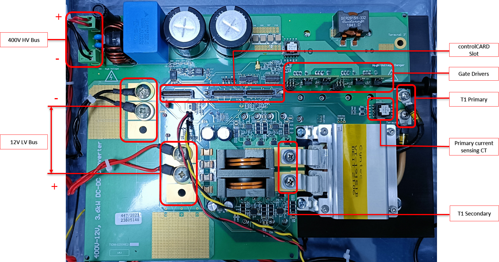
GUID-0B6A5CFD-1D73-4693-A519-3A3333C6F408-low.pngFigure 5-1 TIDM-02009 PSFB Converter Hardware

The key signal connections between the controlCARD and the base board are listed in the Key Signal Connections. The HSEC pin number is based on the E2 version of the AM263x controlCARD (TMDSCNCD263).

Table 5-1 Key Signal Connections
Signal NameDescriptionConnection to ControlCARDHSEC Pin Number
ePWM-4APWM drive for full-bridge switch Q1EPWM4_A57
ePWM-4BPWM drive for full-bridge switch Q4EPWM4_B59
ePWM-3APWM drive for full-bridge switch Q2EPWM3_A54
ePWM-3BPWM drive for full-bridge switch Q3EPWM3_B56
ePWM-5APWM drive for sync rectifier/push-pull switch Q5EPWM5_A61
ePWM-5BPWM drive for sync-rectifier/push-pull switch Q6EPWM5_B63
VLV-FBLow voltage bus – voltage feedbackADC3_AIN234
ILV-FILTHeavily filtered low voltage current feedbackADC1_AIN218
VHV-FBHigh voltage bus – voltage feedbackADC3_AIN130
IHV-FILTHeavily filtered transformer high voltage winding currentADC4_AIN0
/ADC_CAL0
25

While running the hardware, pin #1 and #2 of J19 in the base board must be shorted with a jumper. 12V power supply must be applied in between pin #9 and#7 of J17 connector only if gating pulses for the Q5, Q6 are to be enabled.