SPRUIU8A March 2020 – August 2021 TMS320F280040-Q1 , TMS320F280040C-Q1 , TMS320F280041 , TMS320F280041-Q1 , TMS320F280041C , TMS320F280041C-Q1 , TMS320F280045 , TMS320F280048-Q1 , TMS320F280048C-Q1 , TMS320F280049 , TMS320F280049-Q1 , TMS320F280049C , TMS320F280049C-Q1
3 Memory Layout
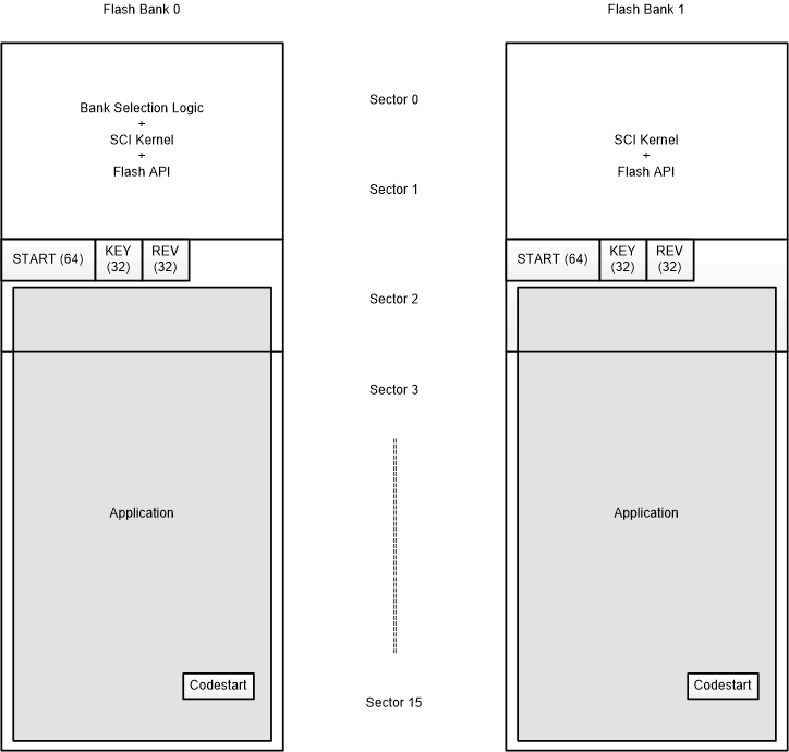
The Flash memory has been partitioned as shown in Figure 3-1.
 Figure 3-1 Flash Memory Contents for Bank 0 and Bank 1
Assuming each Flash bank has 16 sectors, two sectors have been allocated to Static code (code that will not change between applications). This is described in Section 4.
A few locations in sector 2 have been reserved to store the below entries:
- START – when this 64-bit field is set in a specific Flash bank (to 0x5A5A5A5A5A5A5A5A) by the Serial Communications Interface (SCI) Flash Kernel, it indicates that the corresponding Flash bank has been erased (Application sectors) and programming/verification is about to begin. In this example, the START field is located at addresses 0x82000 in BANK0 and 0x92000 in BANK1.
- REV – this represents a 32-bit Firmware revision number that is set by the SCI Flash Kernel which is used by the Bank Selection Logic to determine which the latest image is between Flash bank 0 and 1. REV starts at 0xFFFFFFFF and is decremented on each subsequent Flash programming cycle. Thus, the Bank with the lower revision number is considered the latest one. Firmware revision field is handled by the flash kernel for simplicity. In practice, the last downloaded image may not be the latest firmware version and the application image would contain the firmware version, but that assumption is made with this model where the kernel updates the REV field. In this example, the REV field is located at address 0x82006 in BANK0 and 0x92006 in BANK1. As an example, if the REV in BANK0 is FFFF FFFA, and the REV in BANK1 is FFFF FFF9, BANK1 will be considered the latest firmware and will execute.
- KEY– The image in a bank is considered as valid if this location contains a valid KEY (0x5B5B5B5B). This Key is written to by the SCI Flash Kernel, and is read and tested by the Bank Selection Logic. In this example, the KEY field is located at addresses 0x82004 in BANK0 and 0x92004 in BANK1.
The rest of sector 2 and sectors 3-15 can be used to store the application image. This allows the static code in sectors 0 and 1 to be programmed once, and remain unchanged during LFU.