SPRUIU8A March 2020 – August 2021 TMS320F280040-Q1 , TMS320F280040C-Q1 , TMS320F280041 , TMS320F280041-Q1 , TMS320F280041C , TMS320F280041C-Q1 , TMS320F280045 , TMS320F280048-Q1 , TMS320F280048C-Q1 , TMS320F280049 , TMS320F280049-Q1 , TMS320F280049C , TMS320F280049C-Q1
5 LED Example Application and LFU Flow
This example (flashapi_ex3_live_firmware_update project) is designed to demonstrate LFU with the LED blinking periodically. This is achieved using the Live Device Firmware Update (Live DFU or LDFU) command, which is part of SCI kernel. This is to be used with the Serial Flash Programmer (PC tool).
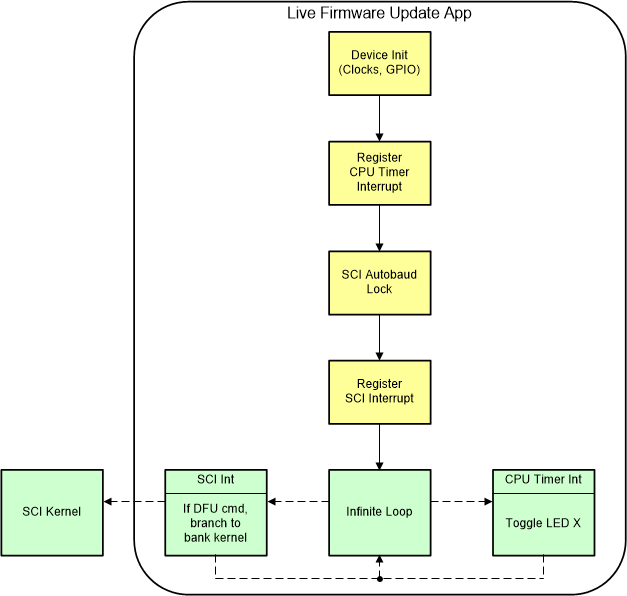
In this example, an SCI auto baud lock is performed and the byte used for auto baud lock is echoed back. Two interrupts are initialized and enabled: SCI Rx FIFO interrupt and CPU Timer 0 interrupt. The CPU Timer 0 interrupt occurs every 1 second; the interrupt service routine (ISR) for CPU Timer 0 toggles an LED based on the build configuration that is running.
- LED1 is toggled with the BANK0_FLASH build configuration. “BANK0” is a pre-defined symbol in this build configuration, and when this symbol is defined, the project sets up GPIOs associated with LED1.
- LED2 is toggled with the BANK1_FLASH build configuration. “BANK1” is a pre-defined symbol in this build configuration, and when this symbol is defined, the project sets up GPIOs associated with LED2.
The application images generated by building the above build configurations are the ones that will be used to illustrate LFU in this document. Note that other than the changes described above between the two build configurations, there are no other differences between the two application images. Hence, this is a relatively simple example for LFU illustration.
The SCI Rx FIFO interrupt is set for a FIFO interrupt level of 10 bytes. The number of bytes in a packet from the Serial Flash Programmer (when using the LDFU command) is 10. When a command is sent to the device from the Serial Flash Programmer, the SCI Rx FIFO ISR receives a command from the 10 byte packet in the FIFO. If the command matches the Live Device Firmware Update (Live DFU) command, then the code branches to the Live DFU function (liveDFU()) located inside of the SCI Flash Kernel (flashapi_ex2_ldfu.c) for the corresponding bank. So if the application on Bank0 is executing, control will pass to liveDFU() on Bank0, located at 0x81000. If the application on Bank1 is executing, control will pass to liveDFU() on Bank1, located at 0x91000. Within this function, execution passes to the ldfuLoad() function in order to erase the appropriate bank, load a hex formatted program (in the appropriate SCI boot format) into flash, and verify the program. Then the watchdog is configured for a reset. At the end, the watchdog is enabled in order for a reset to occur. When the device resets, it boots and loads the new Firmware.
Figure 5-1 depicts the flow of the code at a high level after the code enters main() of the application. For more details, see the flashapi_ex3_live_firmware_update.c located in the flashapi_live_firmware_update project (included in C2000Ware at <C2000Ware>\driverlib\f28004x\examples\flash).
 Figure 5-1 Code Flow After Entering main() of Application