SPRUJ10D May 2022 – September 2023
- 1
- Abstract
- Trademarks
- 1Preface: Read This First
- 2Kit Overview
- 3Board Setup
-
4Hardware Description
- 5.1 Functional Block Diagram
- 5.2 GPIO Mapping
- 5.3 Reset
- 5.4 Clock
- 5.5 Memory Interface
- 5.6 Ethernet Interface
- 5.7 I2C
- 5.8 Industrial Application LEDs
- 5.9 SPI
- 5.10 UART
- 5.11 MCAN
- 5.12 FSI
- 5.13 JTAG
- 5.14 Test Automation Header
- 5.15 LIN
- 5.16 MMC
- 5.17 ADC and DAC
- 5.18 EQEP and SDFM
- 5.19 EPWM
- 5.20 BoosterPack Headers
- 5.21 Pinmux Mapping
- 5References
- 6Revision History
4.6.2 Ethernet PHY #2 - CPSW RGMII/ICSSM
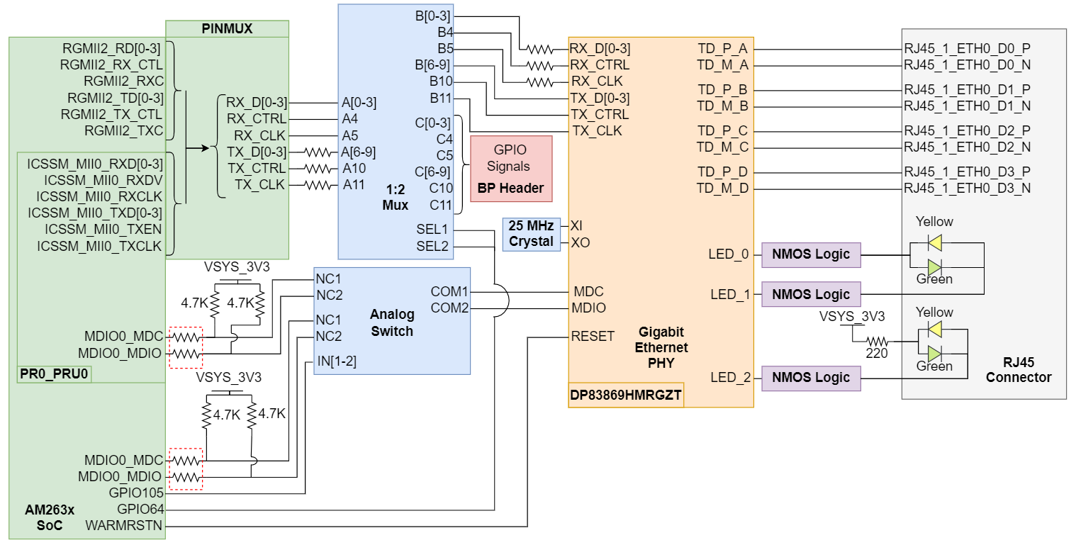
The AM263x LaunchPad utilizes a 48-pin ethernet PHY (DP83869HMRGZT) connected to either CPSW RGMII or one on-die programmable real-time unit and industrial communication subsystem (PRU-ICSS). The RGMII CPSW port and ICSSM are internally pinmuxed on the AM263x SoC. For more information on the internall muxing of signals refer to Pinmux Mapping. The PHY is configured to advertise 1-Gb operation. The ethernet data signals of the PHY are terminated to an RJ45 connector. The RJ45 connector is used on the board for Ethernet 10/100/1000 Mbps connectivity with integrated magnetics and LEDs for link and activity indication.

The Ethernet PHY requires three separate power sources. VDDIO is the 3.3V, system generated supply. There are dedicated LDO's for the 1.1V and 2.5V supplies for the Ethernet PHY.
There are series termination resistors on the transmit clock and data signals located near the SoC. There are series termination resistors on the receive clock and data signals near the Ethernet PHY.
The MDC and MDIO signals from the SoC to the PHY require 4.7KΩ pull up resistors to the 3.3 V system supply voltage for proper operation. There is an analog switch (TS5A23159DGSR) that selects between the CPSW MDIO/MDC and the ICSSM MDIO/MDC signals to be routed to the ethernet PHY.
AM263x internal Pinmux is used to select between CPSW RGMII and ICSSM signals. The signals are then routed to a 1:2 Mux (TS3DDR3812RUAR) that selects between mapping the signals to the Ethernet PHY or the BP headers in the case that the PRU GPIO signals are being used in a BoosterPack application. There is an AM263x SoC GPIO select signal that drives the 1:2 mux.
| GPIO64 | Condition | Function of Mux |
|---|---|---|
| LOW | Ethernet PHY Selected | Port A ↔ Port B |
| HIGH | BoosterPack header Selected | Port A ↔ Port C |
The reset input for the Ethernet PHY is controlled by the WARMRESET AM263x SoC output signal.
The Ethernet PHY uses many functional pins as strap option to place the device into specific modes of operation.
| Functional Pin | Default Mode | Mode in LP | Function |
|---|---|---|---|
| RX_D0 | 0 | 0 | PHY address: 1100 |
| RX_D1 | 0 | 3 | |
| JTAG_TDO/GPIO_1 | 0 | 0 | RGMII to Copper |
| RX_D3 | 0 | 0 | |
| RX_D2 | 0 | 0 | |
| LED_0 | 0 | 0 | Auto-negotiation, 1000/100/10 advertised, auto MDI-X |
| RX_ER | 0 | 0 | |
| LED_2 | 0 | 0 | |
| RX_DV | 0 | 0 | Port Mirroring Disabled |