SSZT535 february 2019 LMR33630 , TPS7A16 , TPS7A47
The efficiency of a low-dropout regulator (LDO) depends on its input voltage and output voltage, since the input current drawn from the power supply will be equal to the current required at the output of the LDO. Therefore, a higher input and output voltage difference in the LDO translates to a lower efficiency value, and vice versa. An LDO with low efficiency translates into power loss and causes heating inside the device.
Sometimes, you are going to need an LDO at the point of load because of its low-noise properties. For example, in an automotive rear camera design, an LDO can provide power to the analog circuitry of the Flat Panel Display (FPD)-Link serializer, which normally requires a 1.8-V rail. As the input voltage rail normally starts from a battery (12 V or 24 V), one way to increase the overall system efficiency is to use a DC/DC converter as the first stage of conversion, followed by an LDO.
Since LDO efficiency depends on the difference between its output and input voltage, another way to increase overall system efficiency is to use a tracking pre-regulator circuit, as shown in Figure 1. In this case, the VOUT of the DC/DC will always be regulated into a fixed amount above the VOUT of the LDO. The circuit in Figure 1 gives you flexibility to dynamically adjust the LDO voltage without adjusting the voltage on the DC/DC converter individually.
The pre-regulator circuit shown in Figure 1 uses TI’s LMR33630 synchronous buck converter and TPS7A1601 LDO evaluation modules (EVMs), with some modifications to the LMR33630 feedback network. The LDO chosen here is a 60-V LDO, but you could also use a lower-voltage LDO such as the TPS7A4701.
 Figure 1 A Positive-tracking
Pre-regulator with the LMR33630 and TPS7A1601
Figure 1 A Positive-tracking
Pre-regulator with the LMR33630 and TPS7A1601In Figure 1, the feedback from the LMR33630 generates a constant current, IFBB, which flows through the feedback network, RFBT and RFBB.
 Figure 2 Hardware
Implementation
Figure 2 Hardware
ImplementationIn this configuration, the VOUT of the DC/DC will follow the VOUT of the LDO according to Equation 1:
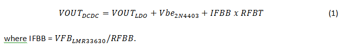
In order to adjust the headroom of the LDO, simply adjust the value of RFBT: IFBB will remain constant.
In the sample design of Figure 1, the TPS7A1601 EVM is set to generate a 5-V output; the LDO output voltage connects to the base of the 2N4403 P-channel N-channel P-channel (PNP) transistor with a 10-kΩ resistor. Since the LMR33630 internal reference voltage is 1 V, the voltage at the VFB of the LMR33630 is also regulated at 1 V.
Following Equation 1, the value of IFBB = 1 V/10 kΩ = 0.1 mA. The Vbe of the 2N4403 is approximately 0.6 V:
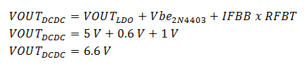
In general, the LMR33630 output voltage will be about 1.6-V higher than the LDO output voltage; this is the LDO headroom.
The waveforms in Figure 3 and Figure 4 illustrate the performance of the system.
 Figure 3 Startup Waveform, with the
LMR33630 Tracking the LDO Voltage
Figure 3 Startup Waveform, with the
LMR33630 Tracking the LDO Voltage") Figure 4 The LMR33630 Tracking the
Up-ramp of LDO Voltage (the LDO Feedback Network Is Injected with a Ramp to
Control Its Output Voltage)
Figure 4 The LMR33630 Tracking the
Up-ramp of LDO Voltage (the LDO Feedback Network Is Injected with a Ramp to
Control Its Output Voltage)As you can see in Figure 4, the TPS7A1601 voltage rmps up with a rise time of 200 µs and the LMR33630 output voltage tracks quite nicely, at 1.6 V above the LDO voltage. Since there is less output current on the LDO, this means that there is only a small load on the LMR33630. Therefore, during the down transition, the LDO voltage ramped down faster than the LMR33630 output voltage (note the time base shown in Figure 5). Once both voltages settle, you can see in Figure 5 that the LMR33630 output voltage is still above the LDO voltage by 1.6 V.
 Figure 5 The LMR33630 Tracking the
Down-ramp of the LDO Voltage
Figure 5 The LMR33630 Tracking the
Down-ramp of the LDO VoltageOne last thing to check is the overall system stability by performing load-transient testing at the output of the TPS7A1601 LDO. Figure 6 is a scope capture showing a load transient at the output of the TPS7A1601 LDO from 0 to 100 mA. The scope shot shows that even during a load transient, the LMR33630 tracks the TPS7A1601 LDO output voltage.
") Figure 6 Load-transient Waveform for
the TPS7A1601 from 0 to 100 mA (VOUTDCDC and VOUTLDO Are AC-coupled)
Figure 6 Load-transient Waveform for
the TPS7A1601 from 0 to 100 mA (VOUTDCDC and VOUTLDO Are AC-coupled)As you can see, it is possible to employ a tracking pre-regulator to increase the overall system efficiency of an LDO with a DC/DC converter by minimizing the difference between the input and output voltage of the LDO. In part two of this series, we’ll use a similar technique to create a tracking pre-regulator for a negative output LDO.