SSZT816 january 2018 DS160PR410
It’s been quite a while since the current PCI Express (PCIe) Gen 4 specification became official. The PCIe Gen 4 specification reached version 1.0 in late 2017 while PCIe Gen 5 reached version 1.0 in early 2019. PCIe Gen 4 doubles the available data rate to 16 Gbps and provides backward compatibility with previous PCIe generations. By using the same 128/130 encoding scheme and equalization training, system architects don’t expect conversion issues as the industry jumps to the updated standard.
Doubling the data rate does impose some distance limitations on the native channel length, especially with standard FR4-printed circuit board material. Improving the connector and enhancing PCIe receiver capabilities has translated into a larger attenuation budget for the PCIe channel. Even with the larger attenuation budget, the maximum channel length tends to be shorter for a PCIe Gen 4-compliant link. To counteract increased attenuation, a much higher percentage of PCIe Gen 4 systems are using link extension devices and/or improved board materials. The term link extension can describe two types of signal conditioning devices, as shown in Table 1.
| PCIe Linear Redriver | PCIe Retimer |
|---|---|
| Low power consumption solution (no heat sink is required). | High power consumption solution (most cases require heat sink). |
| Ultra-low latency (100 ps). | Medium latency (less than or equal to 64 ns based on PCIe Gen4 Specification Requirement). |
| Does not participate in link training but is transparent to negotiations between Root Complex (CPU) and Endpoint (EP). (Protocol agnostic) | Fully participates in link training with Root Complex (CPU) and Endpoint (EP). (Protocol aware) |
| No 100-MHz reference clock is required. | 100-MHz reference clock is required. |
| Helps with insertion loss. | Helps with insertion loss, jitter, crosstalk, reflections and lane-to-lane skew. |
| CTLE is the typical equalization circuit used. | CTLE, DFE and transmitter FIR are typical equalization circuits used. |
| Total solution cost is ≅X. | Total solution cost is ≅(1.3X to 1.5X). |
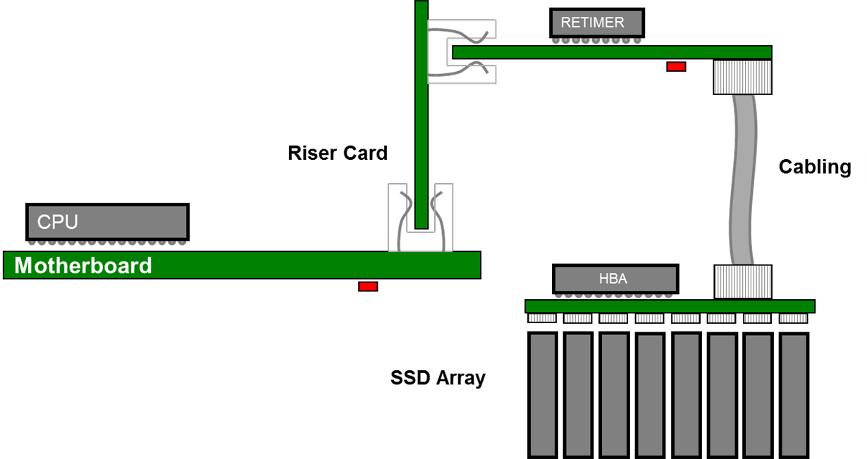
A linear equalizer is an analog-only device designed to boost the incoming signal with continuous time linear equalization (CTLE). This type of gain and link extension is best used for system channels dominated by attenuation due to the physical nature of some server topologies where insertion loss violates PCIe Gen4 specification of 28 dB at 8 GHz by a good margin. An example topology is shown in Figure 1. System components are not designed to handle the increased insertion loss alone even with improved board materials.
 Figure 1 TI Redriver Enabling Channel
Reach beyond Specification Limits
Figure 1 TI Redriver Enabling Channel
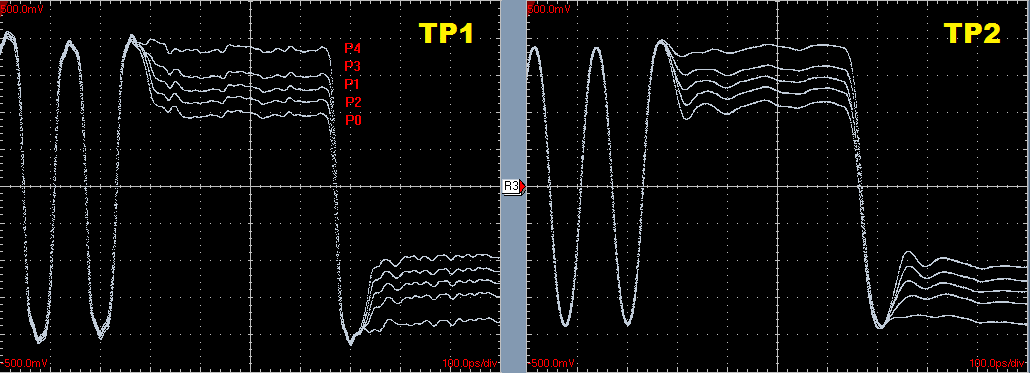
Reach beyond Specification LimitsKey performance metrics for a linear equalizer are a large dynamic voltage range, low additive random jitter and easily controlled AC gain. To demonstrate the performance of linear equalization, a family of PCIe presets, as shown in Figure 2, was captured directly from a 16-Gbps generator (TP1). A channel containing a linear equalizer then used the same signals as inputs. Measurements after the channel and linear equalizer at TP2 show it is possible to completely compensate for high-speed channel losses with linear equalization. Accurate reproduction of the analog waveform content ensures that in-channel equalization will not compromise any digital algorithms used for link equalization training.
 Figure 2 PCIe Tx Preset Family, before
and after a Channel That Includes a Linear Equalizer
Figure 2 PCIe Tx Preset Family, before
and after a Channel That Includes a Linear EqualizerA PCIe retimer is a combination of analog and digital circuits with specific features and requirements to directly interoperate with other PCIe Gen 4 devices. The addition of digital control and protocol awareness enables the retimer to completely reset the system’s jitter budget and handle the full channel attenuation specified in PCIe. This doubles the effective reach of a PCIe system link, enabling a wide variety of system architecture and topology choices, as shown in Figure 3.
 Figure 3 Multi-clock Domain PCIe
Link
Figure 3 Multi-clock Domain PCIe
LinkThe PCIe standard continues to be the primary input/output (IO) interconnect within the server and PC environment. As engineers work to extend PCIe beyond the server to take advantage of its simplicity, scalability and bandwidth, they must also deal with PCIe clock distribution throughout the expanded system. To help alleviate distribution problems, many designs are moving to PCIe implementations that encompass multiple local clock domains. Retimers supporting separate reference clock with independent spread (SRIS) are ideally located to be a clock domain boundary as PCIe signals travel across cables or between server chassis in a rack.
As a recognized system component, a PCIe retimer will engage in equalization training on the upstream and downstream channels. This built-in capability automatically optimizes the signal-conditioning solution for short, medium or long PCIe-compliant channels.
The choice of a signal conditioning solution (Table 2) whether it is a redriver, a redriver with integrated mux/demux, or a protocol-aware retimer will depend on many system factors. Systems that need help to lower the effective channel attenuation between system components can consider the redriver since it is a lower-power, ultra-low latency and low-solution cost alternative to a full retimer implementation. Systems with complex topologies, high levels of attenuation and in need of jitter budget reset are good candidates for a retimer solution.
Additional Resources:
- Learn more about the PCI Express in, “NVME and PCI Express: What’s the Difference.”
- What is linear equalization and why is it needed?
- Check out this PCIe compliance report using an advanced linear equalizer.
- Explore signal conditioners to extend reach in data center and server applications.