SSZT952 september 2017 LMG3410R070 , LMG5200
Design engineers faced with the challenges of reduced space and increased power demands are embracing gallium nitride (GaN) technology. By leveraging new topologies, switching frequencies and magnetic design options, GaN has enabled systems to reach unprecedented levels of power density and efficiency. However, these designs need to meet the industry’s expectation for reliability, availability of proven solutions and cost parity with silicon metal-oxide semiconductor field-effect transistors (MOSFETs).
TI has long been a leader and advocate in developing and implementing comprehensive methodology to ensure long and reliable operation and lifetimes of GaN devices under the harshest operating conditions. To achieve this, the traditional silicon methodology needs to be extended for GaN and its intrinsic characteristics. Additionally, stress testing needs to include the switching conditions of power management, which traditional silicon qualification does not address.
The power electronics industry recently reached an exciting milestone. The Joint Electron Device Engineering Council (JEDEC) announced the formation of a new committee: JC-70 Wide Bandgap Power Electronic Conversion Semiconductors. This committee’s charter is to standardize reliability and qualification procedures, data sheet elements and parameters, and test and characterization methods for GaN as well as silicon carbide (SiC). Having a common standard will enable the power industry to compare and contrast different GaN devices through a single lens. It will also help suppliers better differentiate their solutions and the merits of their technology.
TI is addressing the need for proven and ready-to-use solutions that include:
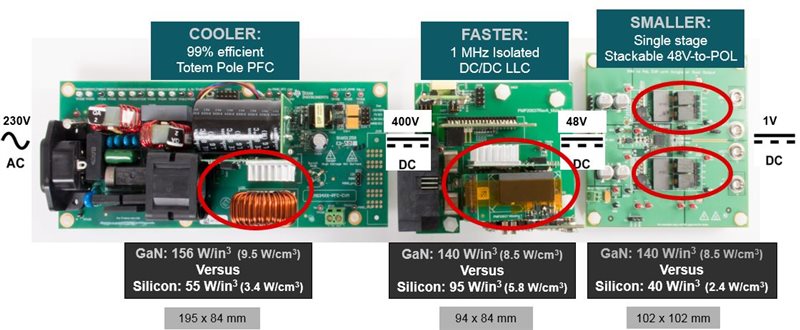
- 99% efficient totem-pole power factor correction (PFC) scalable to 3kW.
- A 1MHz-140W/in3 isolated DC/DC LLC converter.
- A single-stage 48V-to-point-of-load (POL) solution with 4x the power density of MOSFETs.
- A high-density 48V/10A high-frequency three-phase GaN motor drive.
- A three-phase 200V GaN AC servo drive with 99% efficiency.
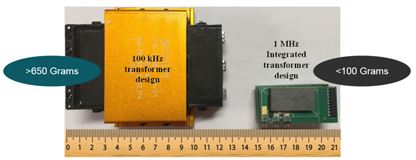
These solutions, as shown in Figure 1, are not just about 2x the power density. In every stage, GaN-based solutions reduce the number and/or size of both passive and active components (Figure 2), heat sinks, cooling requirements and physical space. These savings help you achieve system-cost parity with silicon MOSFETs with at least 2x the power density.
 Figure 1 AC-to-POL Solution with
GaN
 Figure 2 GaN Reduces the Size of
Magnetics
Figure 2 GaN Reduces the Size of
MagneticsAs GaN continues on its path forward, we at Texas Instruments are excited to be part of the journey.
Additional Resources
- Read these TI E2E™ Community blog posts:
- Download these white papers:
- View the Applied Power Electronics Conference 2016 presentation, “Application-Relevant Qualification of Emerging Semiconductor Power Devices.”