SSZTBI2 March 2016 LM5140-Q1
A controller is capable of regulating a maximum output voltage: for example, the LM5140-Q1 regulates a maximum output voltage of 15V. Still, there are many applications where a design engineer would need a regulated voltage above this level, such as for an industrial application where the standard operating bus that provides power for programmable logic controller (PLC) and factory automation equipment is 24V.
In this post, I’ll describe how to design a power supply using the LM5140-Q1 for industrial applications with a 24V output supplying 3A of load current. The LM5140-Q1 was designed for automotive applications where the required regulated output voltages are typically under 8V. With the addition of a few external components, you can use the LM5140-Q1 in industrial applications.
Before beginning the design, the following items should be considered:
- The LM5140-Q1 requires an external 5V bias supply that connects to VCCX.
- An OR’d diode configuration to the buffer amplifier is required to ensure functional operation at startup.
- The absolute maximum VCCX voltage is 6.5V.
- The VOUT pin requires a low impedance input. A resistor voltage divider with a low enough impedance may draw sufficient current that it will affect the system efficiency.
- The LM5140-Q1 internal slope compensation governs the selection of inductor and RSENSE.
Figure 1 shows how to configure the LM5140-Q1 to regulate voltages greater than 15V. Set VO1 to 5V and connect to VCCX. This disables the LM5140-Q1’s internal regulator, reducing the controller’s power dissipation.
 Figure 1 Schematic, LM5140-Q1 with
Extended Output Range External Components
Figure 1 Schematic, LM5140-Q1 with
Extended Output Range External ComponentsYou can configure the LM5140-Q1 with adjustable output voltages using feedback resistors, or with two fixed-output voltage options without using feedback resistors. See the LM5140-Q1 data sheet for additional details.
Using Equation Figure 1, set the output voltage to 24V:
") Figure 2 (1)
Figure 2 (1)where: VREF = 1.2V. See the schematic in Figure 1.
I recommend a starting point for RFB1 between 10kΩ and 20kΩ (Equation Figure 1):
") Figure 3 (2)
Figure 3 (2)218 kΩ is not a standard 1% resistor value so use: 215kΩ
You’ll need two identical voltage dividers for sensing the differential voltage across the current-sense resistor, RCS, and VO2. The input to the buffer amplifier is high-input impedance and will not affect the power-supply efficiency, and the output of the amplifier is low-input impedance capable of driving the VOUT2 pin of the LM5140-Q1.
The LM5140-Q1 CS pin has an absolute maximum voltage rating of 15V. In order to prevent violation of the absolute maximum rating, you’ll use a resistor divider network to reduce the voltage at the CS pin. Use the same divider ratio to reduce the voltage sensed at the input to the buffer amplifier to ensure that the same voltage is sensed at VO2. The common-mode voltage of the buffer amplifier needs to be rated above the voltage seen at its inputs with respect to ground. In this case, the common-mode voltage needs to be above (0.7R/1R) x 24V = 16.8V.
Either VO1 or VO2 – or both – can use the external circuit described. Use an external bias supply to provide power to the LM5140-Q1 VCCX pin.
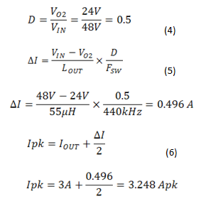
To calculate the output inductor, LOUT, use the following design steps starting with Equation Figure 1, which assumes a 30% inductor-ripple current:
") Figure 4 (3)
Figure 4 (3)where LX is 1.0 +/-0.25 and FSW is the LM5140-Q1’s oscillator frequency (440kHz).
Thus, I selected a 55µH inductor for this application.
Lower inductor values increase the peak-to-peak inductor current, minimize size and cost, and improve transient response. However, lower inductor values reduce efficiency due to higher root mean square (RMS) currents.
Higher inductor values decrease the peak-to-peak inductor current and increase efficiency. You may need larger output capacitors to meet a given transient-response requirement.
Current-sense Resistor
To calculate the current-sense resistor value, multiply the maximum output current (IOUT) by 120% to ensure that the current limit does not affect full load operation: 120% of 3.248 ampire’s peak (Apk) is 3.89Apk.
The voltage dividers attenuate the differential voltage between the CS pin and VOUT pin. This affects the internal slope compensation and current-limit set point. For a 24V output, the external resistors used in the voltage dividers have a ratio of 0.7. Equation Figure 1 accounts for this attenuation:
") Figure 5 (7)
Figure 5 (7)where VCS is the current-limit set point, which for the LM5140-Q1 is 75mV, and A is the resistive divider network attenuation factor, which is 0.7.
The LM5140-Q1 was designed for automotive applications where the required regulated output voltages are typically under 8V. With the addition of a few external components, and by using the design approach detailed in this blog, you can use the LM5140-Q1 controller in industrial applications that require higher output voltages exceeding the absolute maximum voltage ratings of the CS and VOUT pins.
Additional Resources
- Open the “LM5140-Q1 Evaluation Module User’s Guide.”