SSZTC39 october 2015 BQ24250 , CC2564 , DLP2010NIR , DLPA2005 , DLPC150 , TM4C1297NCZAD
Since its announcement in March, developers have been eagerly anticipating the day when they can get their hands on the DLP®NIRscan™ Nano Evaluation Module (EVM). And with good reason. The EVM rapidly evaluates the industry's first fully programmable micro-electro mechanical systems (MEMS) chipset for ultramobile analysis for a 900-1,700 nm wavelength range and it does so with 6,000:1 signal-to-noise ratio (typical) and while fitting in the palm of your hand.
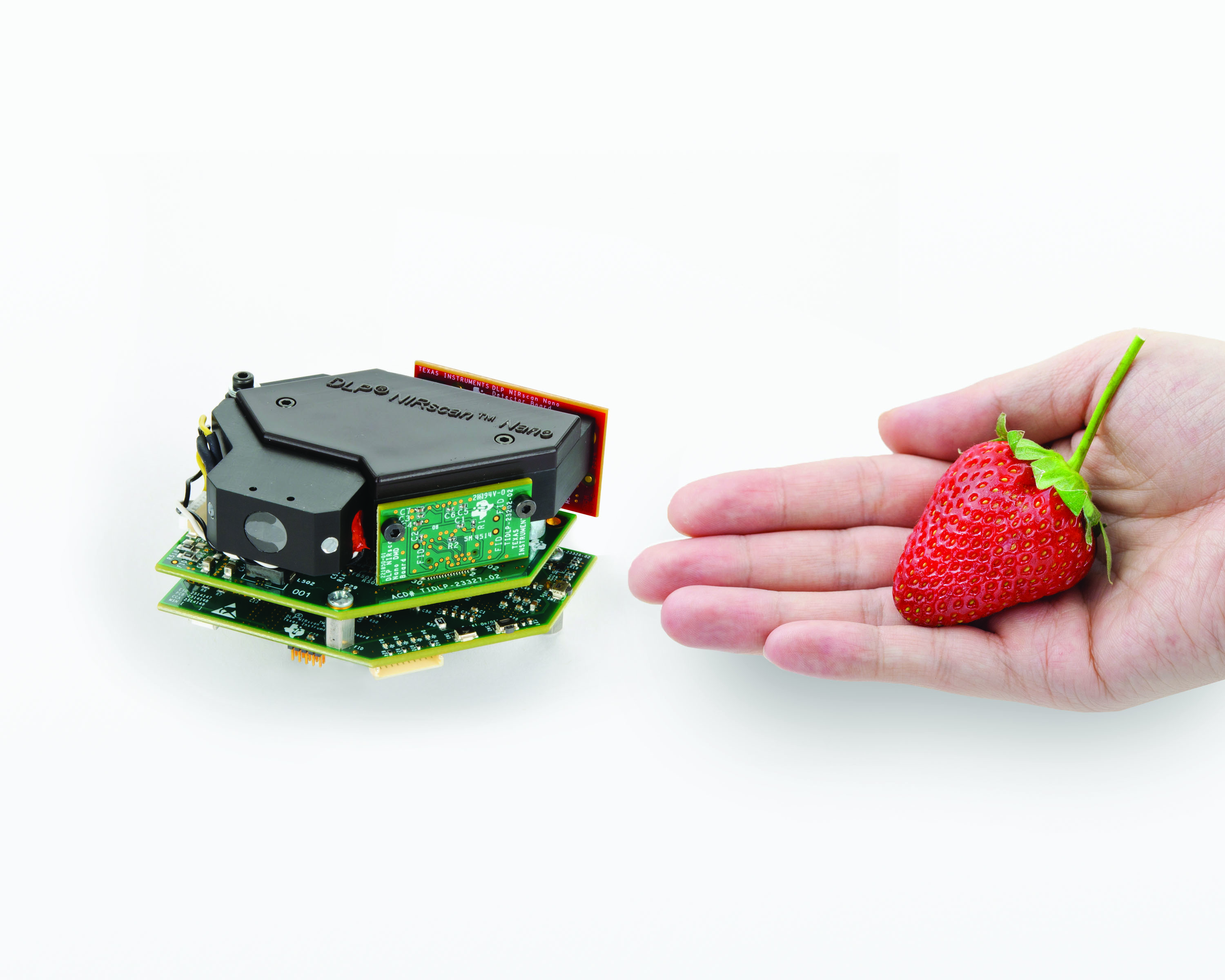
The chipset consists of the DLP2010NIR digital micromirror device (DMD), the DLPA2005 integrated power management and the DLPC150 controller. This potent combination of technology provides low power consumption, programmable high-speed patterns and the latest high-tilt 5.4μm pixel size for use in compact optical designs.
The DLP2010NIR DMD is the smallest, most efficient DLP chip, specifically for handheld near-infrared (NIR) sensing application areas, including spectrometers and chemical analyzers. Application areas include farming, food and drink, petrochemical, health, and skin care industries. Coupled with the Bluetooth® and Bluetooth low energy-enabled DLP NIRscan Nano EVM, designers can prototype portable analyzers to accelerate the development of ultramobile spectrometers.
What you should know about the DLP2010NIR chip include:
- The two-dimensional micromirror array combined with a single point detector provides a lower cost and greater signal capture than linear array systems.
- A wide NIR-window transmittance of 700-2,500 nm enables accurate spectral analysis and the measurement of a variety of materials.
- Its small size and TRP pixel architecture allow for compact, side illuminated optical engine designs, suitable for handheld or embedded systems.
- The DMD's programmable high-speed 854 x 480 micromirror array allows advanced filtering for fast measurements in handheld applications.
What you should know about the DLP NIRscan Nano EVM
- Industry-leading cost point for high precision analytics makes it accessible to developers
- High-resolution wavelength range and pocket-sized form factor complements its predecessor, the DLP NIRscan EVM.
- Bluetooth and Bluetooth low energy functionality of the embedded TI dual-mode Bluetooth CC2564 wireless network processor module provides iOS and Android™ app developers the ability to create apps to wirelessly connect to the EVM platform.
- The TI Tiva™ TM4C1297NCZAD microcontroller enables highly connected products with its integrated ARM® Cortex®-M4 CPU, 1MB flash, 256KB RAM, 10 I2Cs, eight UARTS, four QSPIs, USB 2.0 and much more.
- When adding a battery, the evaluation module has efficient charging with the bq24250, an I2C controlled or standalone 2-A single-cell switch-mode USB charger that charges battery fast and efficiently with great flexibility.
TI maintains an extensive ecosystem of design houses to accelerate end-product development. The DLP Design Network provides developers a diverse network to support their hardware and software integration, optics design, system integration, prototyping, manufacturing services, and turnkey solutions structured to support current and evolving customer needs.
To begin working with DLP technology, visit our Getting Started page, or watch this video demonstrating the application areas for the DLP2010NIR and NIRscan Nano EVM.