SSZTCL0 june 2015 ADC12J4000
In my previous post, I talked about why you might want to use Radio frequency (RF) sampling data converters to handle higher bandwidths in a design. Data converters that operate directly in the RF bands without the additional circuitry of mixers and local oscillators are very alluring. Plus, it’s possible to sample at 4GSPS and beyond.
But wait! How can you transfer digital data to the field-programmable gate array (FPGA) or processor at those speeds? A traditional low-voltage differential signaling (LVDS) or complementary metal-oxide semiconductor (CMOS) interface is not capable of operating that fast. A JESD204B serialized interface is more common; however, a 12-bit converter sampling at 4GHz within the interface could require 80Gbps of data across the channel. This is no small feat. It requires a combination of high-speed serializer/deserializer (SERDES) transceivers and a large number of lanes. This taxes the capability, power constraints and size of the device.
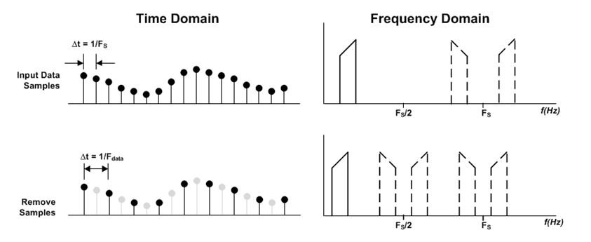
But it is possible to reduce the input data rate by decimation. Decimation is a simple technique where you eliminate sample points from the data stream to reduce the data rate. Figure 1 illustrates a decimate-by-2 operation. Does this technique distort the waveform and lose information? Not exactly. The information is still intact; the drawback is that the decimation operation creates additional images. A decimate-by-2 will introduce images centered at half the sampling-rate point (Fs/2). The decimation process is accompanied by a digital filter to eliminate these images.
A decimate-by-2 function is equivalent to a data converter operating at half rate, with an analog antialiasing filter operating at half the bandwidth. You can also cascade multiple decimate-by-2 stages together to reduce the input data rate to the desirable level.
 Figure 1 Decimation in the Time Domain
and Frequency Domain
Figure 1 Decimation in the Time Domain
and Frequency DomainSo what’s the penalty for this approach? The reduction in data rate will limit the system’s bandwidth capability. Shannon’s sampling theorem still applies. If a 4GSPS device is decimated by 8, for example, the resulting input data rate would be 500MHz, which can support a signal bandwidth of 250MHz.
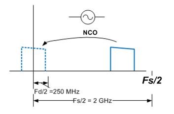
Another useful digital feature is a numerically controlled oscillator (NCO). An NCO is a programmable oscillator that can digitally move the signal captured to a digital baseband location. A common approach is to capture the signal in the RF band and use the NCO to move the signal to zero IF (ZIF). Figure 2 illustrates this approach. The signal can be located at any arbitrary RF frequency and moved down to a known location. Once centered at 0Hz, the maximum data rate required is contingent only on the signal bandwidth. The rule of thumb is to select the output sampling rate based on your RF frequency of operation and to select the input data rate based on the maximum signal bandwidth.
 Figure 2 Example of an NCO
Downconverting Operation
Figure 2 Example of an NCO
Downconverting OperationThe ADC12J4000 RF sampling analog-to-digital converter operates at a sampling rate of 4GSPS. This device uses the JESD204B serialized data interface. It includes decimation modes up to 32x and also has an NCO. Engaging the decimation and NCO allows you to keep the maximum output sampling rate while reducing the input rate based on signal-bandwidth requirements or the processor’s serialization speed limitation.
Come back next month, when I’ll discuss how data-converter aliasing can be your friend.
Additional Resources
- View a video on How to sample and decimate frequencies with ADC12J4000.
- Learn more about the JESD204B interface for high-speed analog-to-digital converters (ADCs).
- See all posts in RJ Hopper’s RF sampling blog series.