SSZTCN5 june 2015 SN65LVDS4

Welcome back to the Get Connected blog series on Analog Wire. In my previous post, I discussed how you can use low-voltage differential signaling (LVDS) to extend the reach of your serial peripheral interface (SPI) communication bus. In this post, I’ll look at using an LVDS receiver as a high-speed comparator, which can be useful in applications where the output from the crystal oscillator is not optimal, or in a photo-detector circuit in a factory setting.
In applications that require a clock to be distributed across a backplane, cable assembly, or even a complex or large motherboard, the clock edges will suffer from the degrading effects of the medium. The product of these effects may be a clock that looks more like a sine wave than a square wave. The impaired clock may be unusable at this point to the end device, meaning that additional internal design team meetings and board spins are soon to follow.
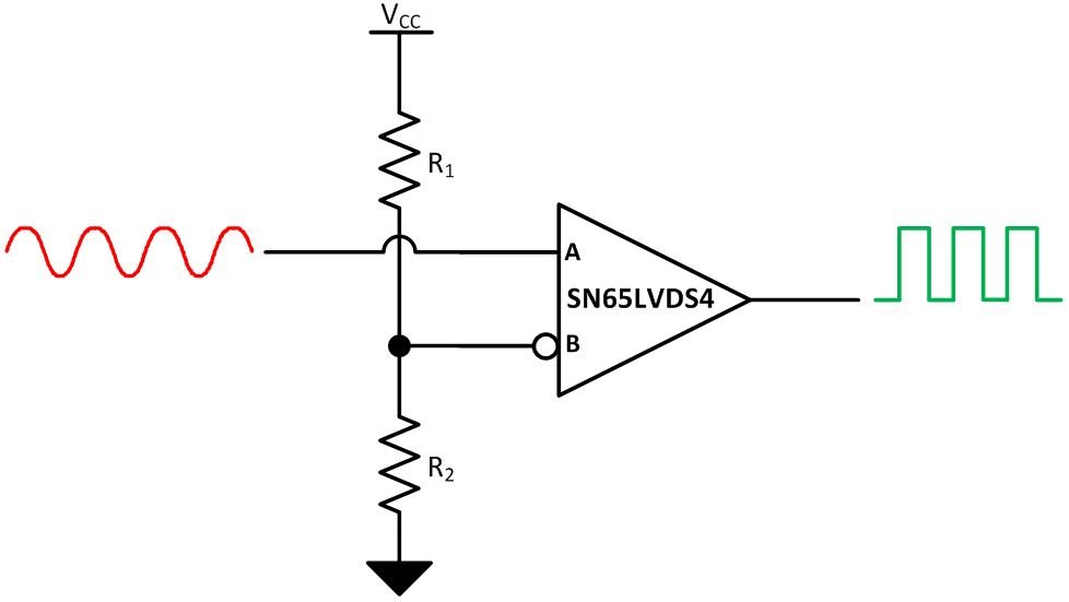
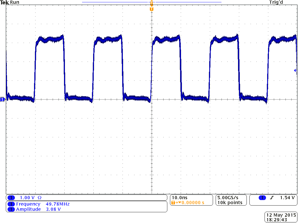
A simple workaround for this problem is to configure an LVDS receiver as a high-speed comparator by placing a static common-mode voltage on one of the inputs and driving the impaired signal into the opposite input. The product of this LVDS implementation is a cleaned-up clock that swings full rail and can now be distributed to the end devices. Figure 1 depicts the LVDS circuit design, while Figure 2 shows the output of the SN65LVDS4 at 50 MHz. The B input is tied to a static 50 mV, and the A input swings from 0 to 100 mV.
 Figure 1 Using an LVDS receiver to
improve oscillator edges
 Figure 2 output at 50 MHz
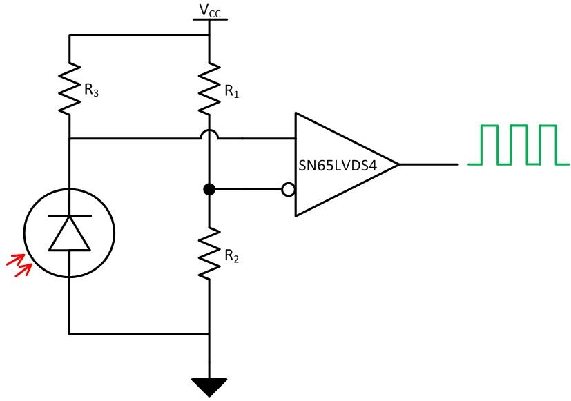
Another application where an LVDS receiver can be used as a high-speed comparator is in an infrared light photo-detector circuit. A photo diode is reverse-biased, and the leakage current through the diode differs based on whether there is light present (IL) or not present (ID) on the diode. Figure 3 shows an example of this LVDS circuit design.
 Figure 3 Photo-detector circuit design
using an LVDS receiver
Figure 3 Photo-detector circuit design
using an LVDS receiverFor this example, let’s say that IL is 30 µA and ID is 5 nA. If the R3 value is 100 kΩ, you can use the always faithful Ohm’s law to calculate the high- and low-level voltage as 3 V and 500 mV, respectively. The reference voltage on the B input of the receiver is VCC/2. When the light is blocked, you will have a dark (ID) situation, and a low level will be registered out of the SN65LVDS4 receiver’s R pin. When the light is not blocked, there is a light (IL) situation, and a high level will be registered out of the SN65LVDS4 receiver’s R pin. A circuit like this may be useful in a factory setting where cans or bottles are flying by a sensor in a bottling plant, and a simple counter is needed to measure productivity.
In my next post, I’ll discuss how a multipoint LVDS (MLVDS) device with extended electrostatic discharge (ESD) performance will help you meet the International Electrotechnical Commission (IEC) 61000-4-2 specification. Leave a comment below if you’d like to hear more about anything discussed in this post, or if there is an interface topic you'd like to see in the future.