TIDT192 October 2020
2.3 Frequency Response
Frequency responses are taken with directly-supplied DC voltage across input capacitors C100 and C108 (that is, VBUS to PGND). 5 V is applied to PSON, Current PWM and Voltage PWM voltage applied differently for different current and voltage regulation settings.
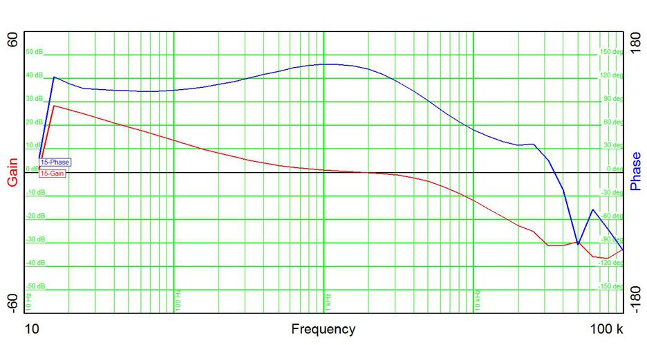 Figure 2-5 Constant Voltage Loop at
200-VDC Input and 24-V, 12-A Output
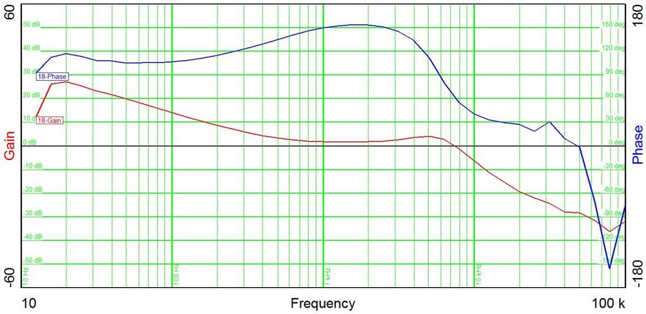 Figure 2-6 Constant Voltage Loop at
370-VDC Input and 24-V, 12-A Output
 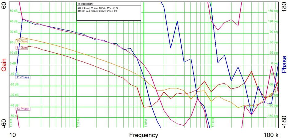 Figure 2-7 Constant Current Loop at
200-VDC Input With Constant Resistor Load.
 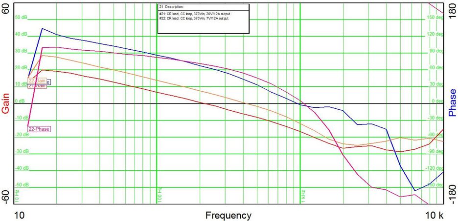 Figure 2-8 Constant Current Loop at
370-VDC Input With Constant Resistor Load.
 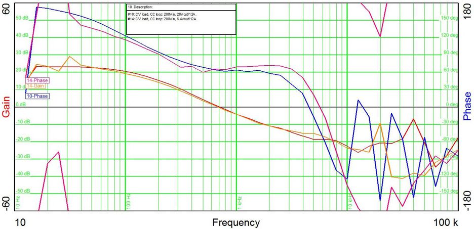 Figure 2-9 Constant Current Loop at
200-VDC Input With Constant Voltage Load.
 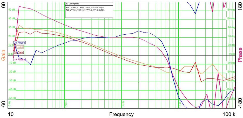 Figure 2-10 Constant Current Loop at
370-VDC Input With Constant Voltage Load.