TIDT205 February 2021
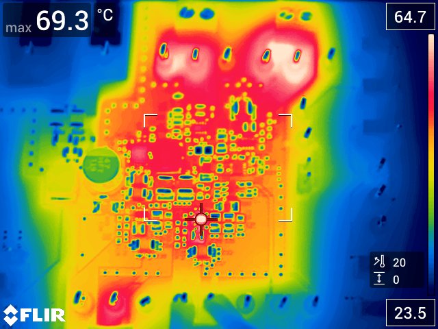
3.4 Thermal Image
The thermal image (with no airflow) was taken with all rails enabled and loaded to their maximum loads. Power resistors were soldered onto the 3V3 LDO, 1V8, 3V3 buck, and 1V35 rails for their loads, and the 1V175 rail was loaded using an electronic load.
Note:
Load each converter using their output testpoints and not the output terminal blocks. The testpoints cut into the plane that the current is traveling through, decreasing the effective area that the current is flowing through on the way to the load connector. If the converters are loaded using the terminal blocks, you may see inaccurate thermal results.
 Figure 3-11 Board Top Thermal Image (VIN = 13.5 V, All Rails at Maximum Load)