TIDT226 April   2021


  1. 1Description
  2. 2Test Prerequisites
    1. 2.1 Voltage and Current Requirements
    2. 2.2 Required Equipment
  3. 3Testing and Results
    1. 3.1 Thermal Images
    2. 3.2 Efficiency and Power Dissipation Graph
    3. 3.3 Efficiency and Power Dissipation Data
    4. 3.4 Cross-Load Voltage Regulation
    5. 3.5 Voltage Regulation Graph
  4. 4Waveforms
    1. 4.1 Start-up Sequence
    2. 4.2 Switch Node
    3. 4.3 Output Voltage Ripple
    4. 4.4 Load Transients

Start-up Sequence

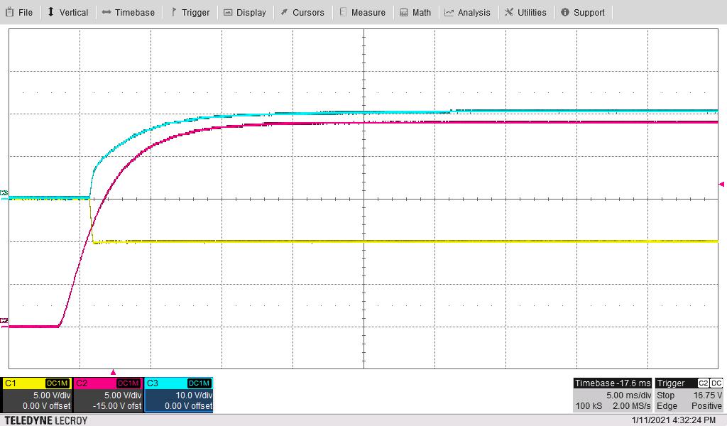
The following waveform shows the output voltage start-up waveform (20 V in Blue and –4 V in Yellow) after the application of 24-V input (Red) with each output loaded to 0 mA.
GUID-20210219-CA0I-6RB9-BN0N-1JZSPVKDW2SN-low.jpg
Vin and –4 V: 5 V/div, 20 V: 10 V/div, 5 ms/div, 750 MHz BWL
Figure 4-1 Output Voltage Start-up Waveform

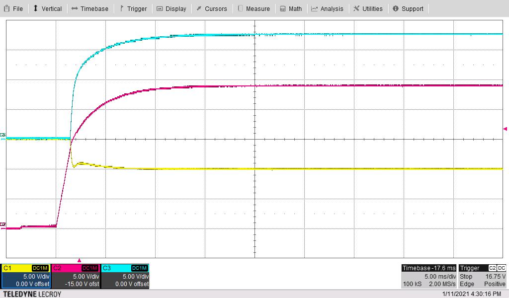
The following waveform shows the output voltage start-up waveform (+20 V in Blue and –4 V in Yellow) after the application of 24-V input (Red) with each output loaded to 100 mA.
GUID-20210219-CA0I-QRQW-CTKW-1MRJ6PZP1PG0-low.jpg
5 V/div, 5 ms/div, 750 MHz BWL
Figure 4-2 Output Voltage Start-up Waveform

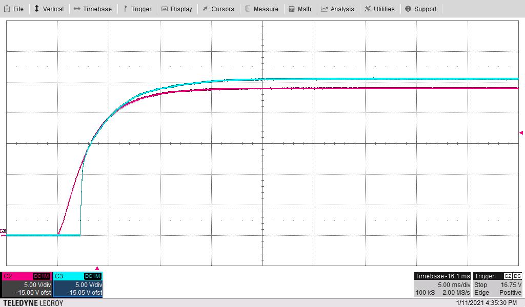
The following waveform shows the total rectified secondary output voltage start-up waveform (Blue) after the application of 24-V input (Red) with each output loaded to 0 mA.
GUID-20210219-CA0I-Q2QP-HCMP-GM0ZXJCNVRPM-low.jpg
5 V/div, 5 ms/div, 750 MHz BWL
Figure 4-3 Total Rectified Secondary Output Voltage Start-up Waveform

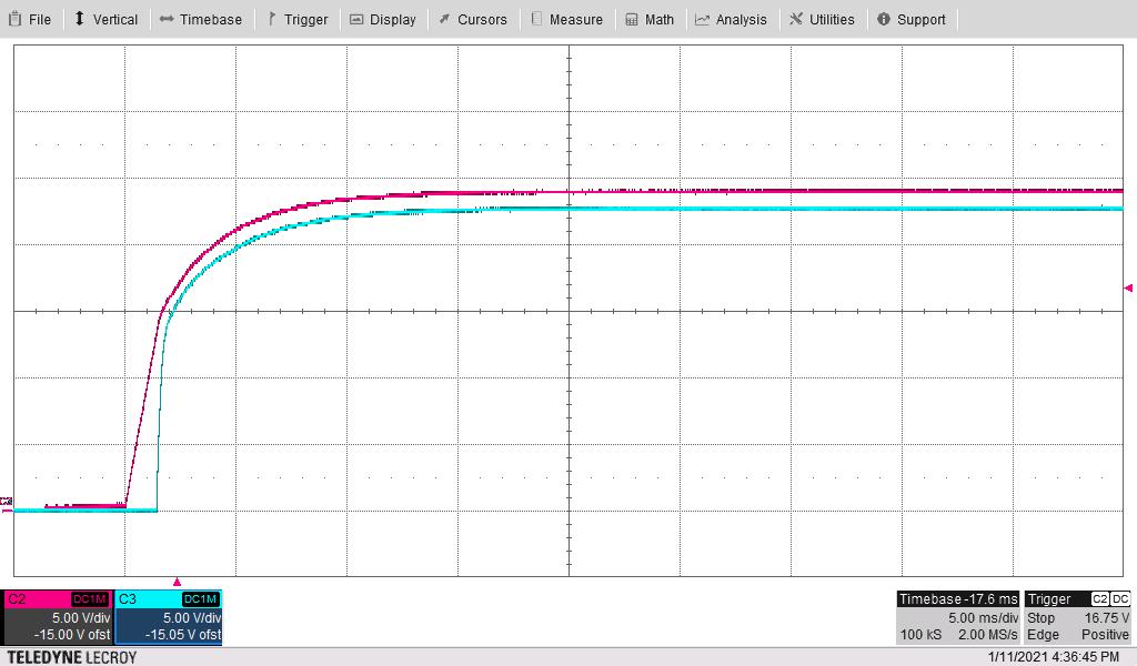
The following waveform shows the total rectified secondary output voltage start-up waveform (Blue) after the application of 24-V input (Red) with each output loaded to 100 mA.
GUID-20210219-CA0I-GBCQ-TGDG-K8TZ3DN5JVR0-low.jpg
5 V/div, 5 ms/div, 750 MHz BWL
Figure 4-4 Total Rectified Secondary Output Voltage Start-up Waveform