TIDT226 April   2021


  1. 1Description
  2. 2Test Prerequisites
    1. 2.1 Voltage and Current Requirements
    2. 2.2 Required Equipment
  3. 3Testing and Results
    1. 3.1 Thermal Images
    2. 3.2 Efficiency and Power Dissipation Graph
    3. 3.3 Efficiency and Power Dissipation Data
    4. 3.4 Cross-Load Voltage Regulation
    5. 3.5 Voltage Regulation Graph
  4. 4Waveforms
    1. 4.1 Start-up Sequence
    2. 4.2 Switch Node
    3. 4.3 Output Voltage Ripple
    4. 4.4 Load Transients

Output Voltage Ripple

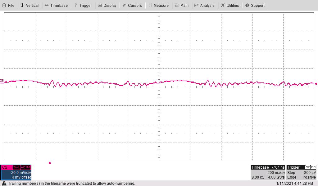
The following waveform shows the 20-V output ripple voltage (AC coupled) measured across C4. The input voltage is 24 V and the 20-V and –4-V outputs are loaded to 100 mA each.
GUID-20210219-CA0I-DGQP-T38B-D39CZNLVM2MK-low.jpg
20 mV/div, 200 ns/div, 20 MHz BWL
Figure 4-11 Output Ripple Voltage, 20 V (AC Coupled)

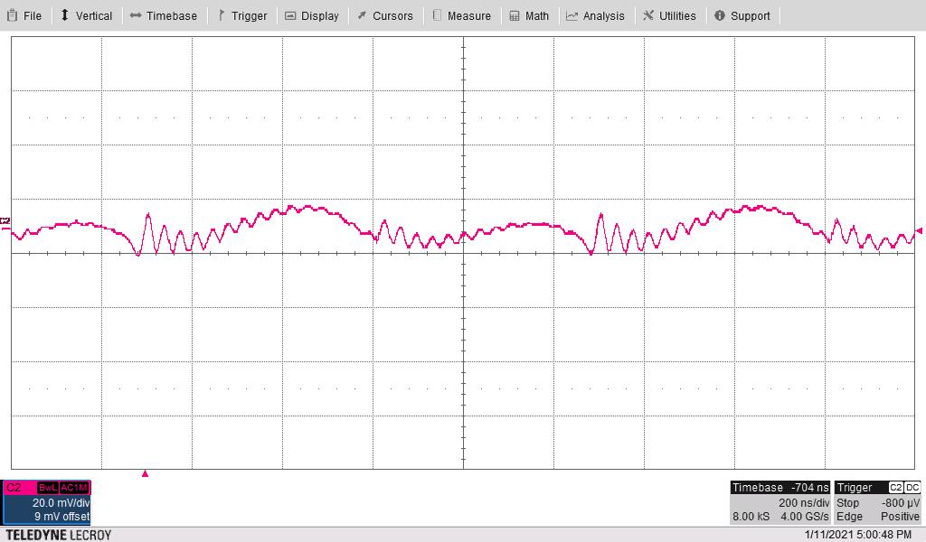
The following waveform shows the 20-V output ripple voltage (AC coupled) measured across C4. The input voltage is 24 V and the 20-V and –4-V outputs are loaded to 300 mA each.
GUID-20210219-CA0I-HJLW-WBMX-T7S5VL1MMWFP-low.jpg
20 mV/div, 200 ns/div, 20 MHz BWL
Figure 4-12 Output Ripple Voltage, 20 V (AC Coupled)

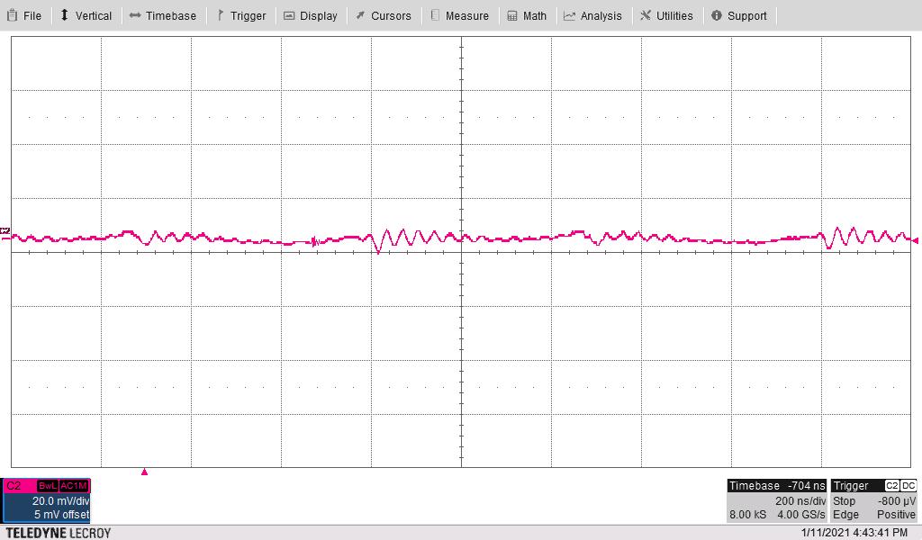
The following waveform shows the –4-V output ripple voltage (AC coupled) measured across C5. The input voltage is 24 V and the 20-V and –4-V outputs are loaded to 100 mA each.
GUID-20210219-CA0I-KBQ7-TNHX-WBWLJFMNCMSL-low.jpg
20 mV/div, 200 ns/div, 20 MHz BWL
Figure 4-13 Output Ripple Voltage, –4 V (AC Coupled)

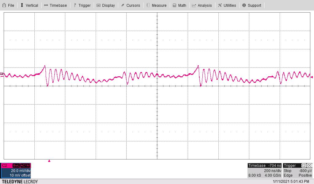
The following waveform shows the –4-V output ripple voltage (AC coupled) measured across C5. The input voltage is 24 V and the 20-V and –4-V outputs are loaded to 300 mA each.
GUID-20210219-CA0I-P0SQ-WSS6-SBL5X2G6JTMK-low.jpg
20 mV/div, 200 ns/div, 20 MHz BWL
Figure 4-14 Output Ripple Voltage, –4 V (AC Coupled)