TIDT242 November 2022
2.3 Thermal Images
The thermal images are shown in the following
figures. The ambient temperature is 25°C, and the thermal images
were taken with 13.5-V input and all outputs at a full load of 3 A.
The controller was operated for approximately 30 minutes before
thermal images were taken to ensure the thermal steady state was
reached. The board is 4-layer PCB, the copper of the top and bottom
layers is 2 oz, and the copper of middle layers is
1 oz.
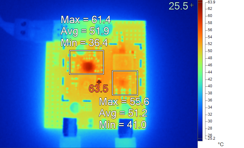 Figure 2-2 Top Side Thermal Image,
VPA_BUS = VPB_BUS = 5 V
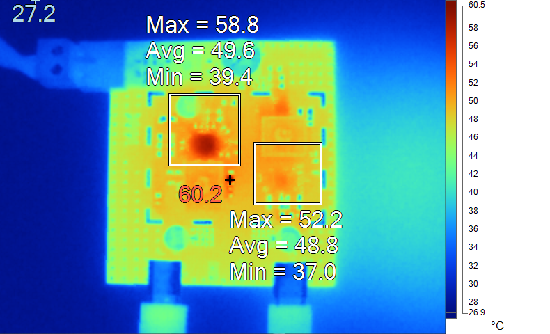 Figure 2-4 Top Side Thermal Image,
VPA_BUS = VPB_BUS = 9 V
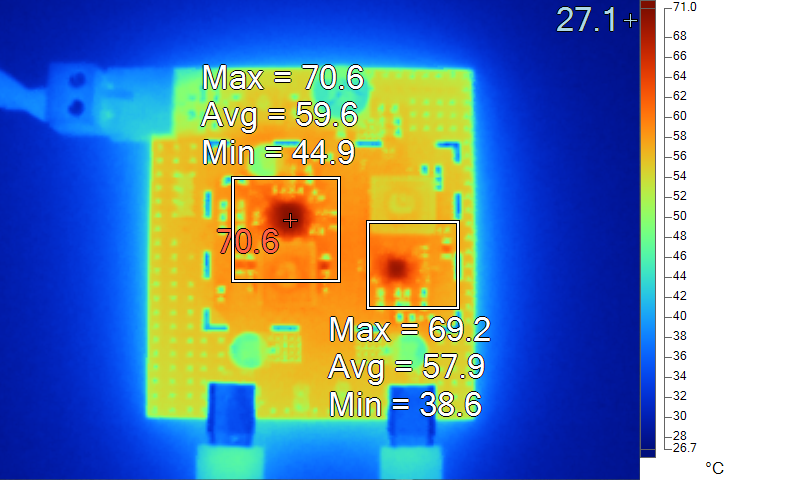 Figure 2-6 Top Side Thermal Image,
VPA_BUS = VPB_BUS = 15 V
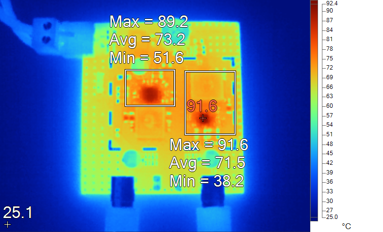 Figure 2-8 Top Side Thermal Image,
VPA_BUS = VPB_BUS = 20 V
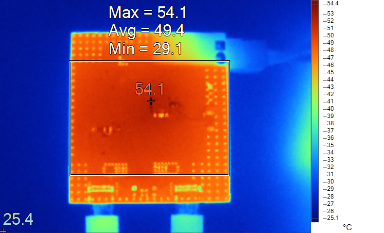 Figure 2-3 Bottom Side Thermal Image,
VPA_BUS = VPB_BUS = 5 V
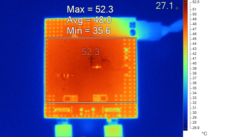 Figure 2-5 Bottom Side Thermal Image,
VPA_BUS = VPB_BUS = 9 V
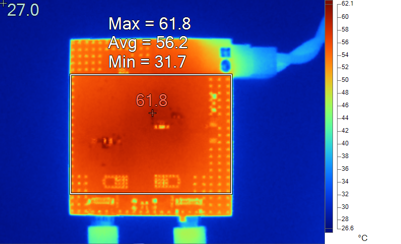 Figure 2-7 Bottom Side Thermal Image,
VPA_BUS = VPB_BUS = 15 V
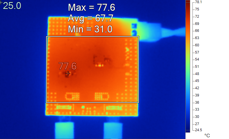 Figure 2-9 Bottom Side Thermal Image,
VPA_BUS = VPB_BUS = 20 V