TIDUES0E June 2019 – April 2024 TMS320F28P550SJ , TMS320F28P559SJ-Q1
- 1
- Description
- Resources
- Features
- Applications
- 6
- 1System Description
- 2System Overview
- 3Circuit Description
- 4Hardware, Software, Testing Requirements, and Test Results
- 5Design Files
- 6Related Documentation
- 7Terminology
- 8About the Author
- 9Revision History
4.4.2 Lab 2
In the lab 2 build, the board is excited in
open-loop fashion with a specified frequency (100 kHz) and phase shift. The phase
shift can be changed through the watch window. The phase shift is controlled with
the DAB_pwmPhaseShiftPrimSec_pu variable. This build verifies the
sensing of feedback values from the power stage, operation of the PWM gate driver,
HW protection, and makes sure there are no hardware issues. Additionally, calibrate
the input and output voltage sensing in this build. For the HW test setup see Section 4.2.
- Software Setup for Lab 2
The following defines are set in the
settings.hfile for this build. The settings can be defined by selecting Lab 2: Open Loop PWM with Protection in the drop-down menu of Project Options from PowerSUITE GUI.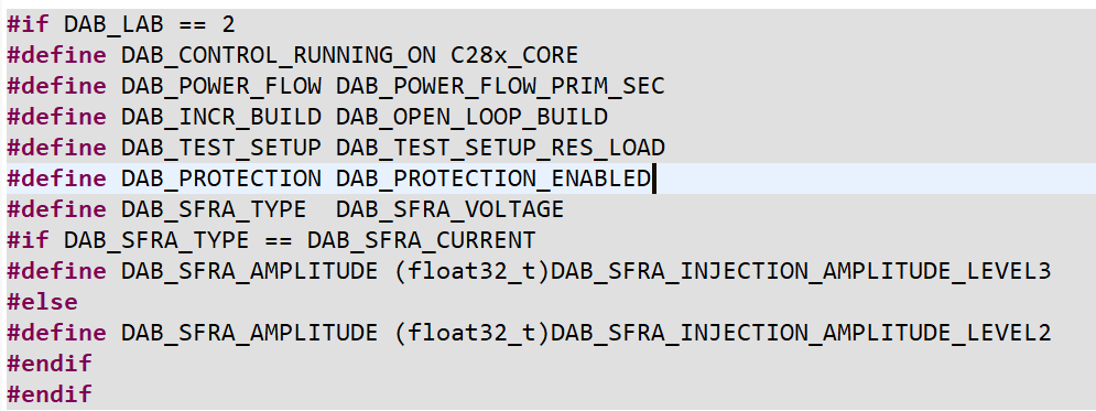 Figure 4-20 Lab 2 Software
Setup
Figure 4-20 Lab 2 Software
Setup- Run the project by clicking the green run button in CCS.
- Populate the required
variables in the watch window by loading JavaScript
setupdebugenv_lab2.jsin the scripting console.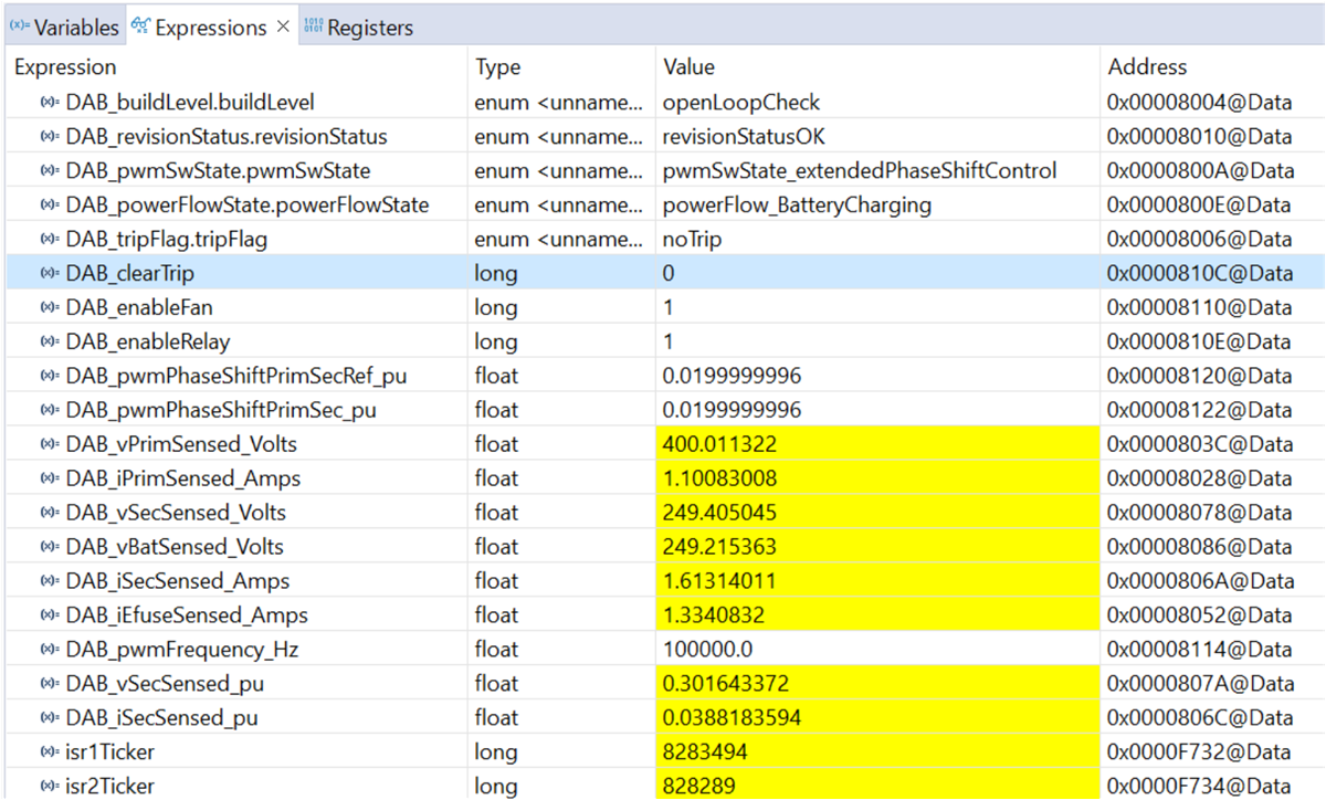 Figure 4-21 Lab 2 Watch
View Configuration
 - In the watch view, check
if the
DAB_vPrimSensed_Volts,DAB_iPrimSensed_Amps, DAB_vSecSensed_Volts, andDAB_iSecSensed_Ampsvariables are updating periodically.Note: Because no power is applied at this point, these variables are close to zero.
Relay and fan validation
- In idle state the auxiliary 12-V power supply needs to consume approximately 700 mA.
- Write a "1" to
DAB_enableRelay. The typical clicking is usually audible and the current consumption needs to increase to approximately 1.14 A. - Write a "1" to
DAB_enableFan. The fans start spinning and the current consumption increases to 1.43 A (here two CFM6015V-154-362 fans are used).
- Power transfer
validation
- Apply a low-input voltage (for example, 50 V)
- Clear PWM trip by writing
"1" into
DAB_cleartrip - Verify that voltage and current appear on the output
- Phase shift can be varied
by modifying
DAB_pwmPhaseShuftPrimSecRef_pu
By default, the
DAB_pwmPhaseShiftPrimSec_puvariable is set to 0.02. Vary this phase shift slowly in steps of 0.002 pu and observe the change in voltage at the output of the converter. Make sure to not increase the phase shift very high as the phase shift can boost the output voltage greater than the input voltage and can lead to breakdown of MOSFETs at the maximum applied voltage.
- Protection validation
Before actual high-voltage and high-power testing, validate the protection features. Validation can also be done at low voltages (for example, 50-V input). The limits for overcurrent and overvoltage protection can be modified from PowerSUITE GUI, see Figure 4-9.
- Primary overcurrent protection:
- Set IPRIM_TRIP to 1 A
- Connect 50-V input voltage
- Enable relays and clear PWM
- Increase phase shift step by step to increase primary current
- Observe trip after 1 A is crossed
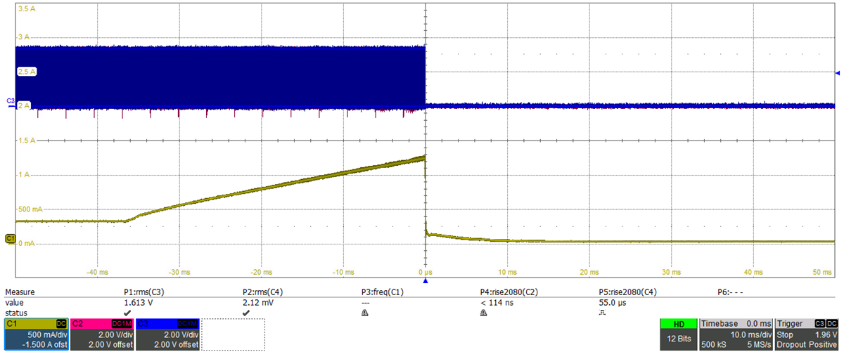 Primary - overcurrent protection, limit set = 1 AFigure 4-22 Lab 2 - Primary Overcurrent Protection
 - Primary tank overcurrent protection
- Set IPRIM_TANK_TRIP to 1.5 A
- Connect 50-V input voltage
- Enable relays and clear PWM
- Increase phase shift step by step to increase primary tank current
- Observe trip after 1.5 A is crossed
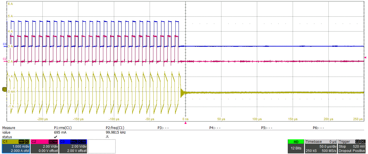 Primary - tank overcurrent protection, limit set = 1.5 AFigure 4-23 Lab 2 - Primary Tank Overcurrent Protection
 - Secondary overcurrent protection
- Set ISEC_TRIP to 1.5 A
- Connect 50-V input voltage
- Enable relays and clear PWM
- Increase phase shift step by step to increase secondary current
- Observe trip after 1.5 A is crossed
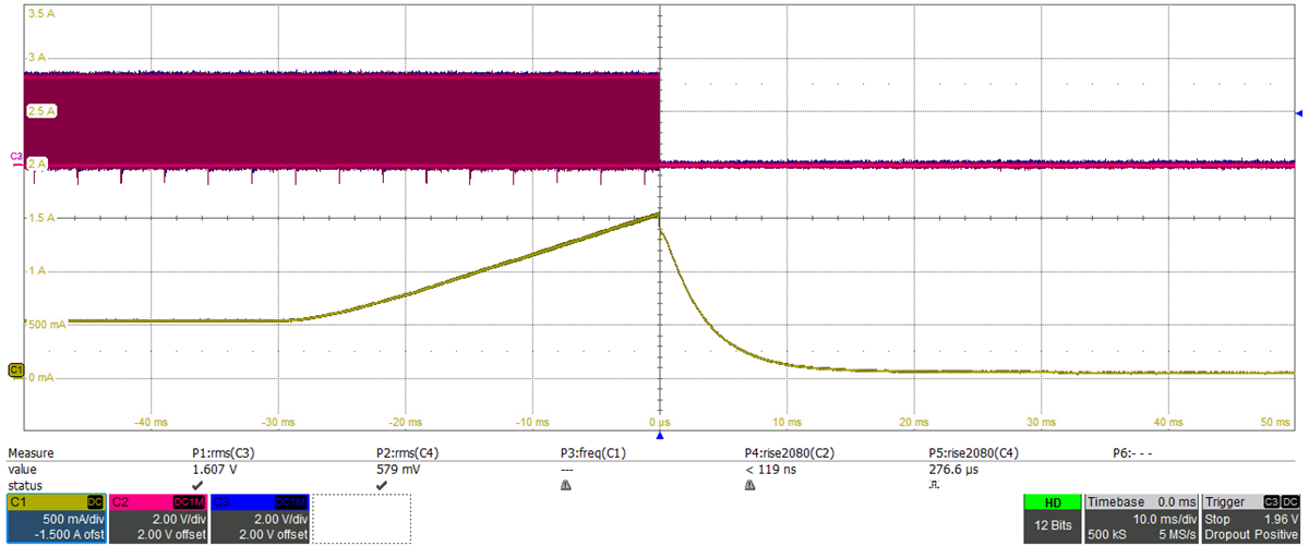 Figure 4-24 LAB 2 -
Secondary Overcurrent Protection
 - Secondary overvoltage
protection
- Set VSEC_TRIP to 40 V
- Connect 50-V input voltage
- Enable relays and clear PWM
- Increase phase shift step by step to increase secondary voltage
- Observe trip after 40 V is crossed
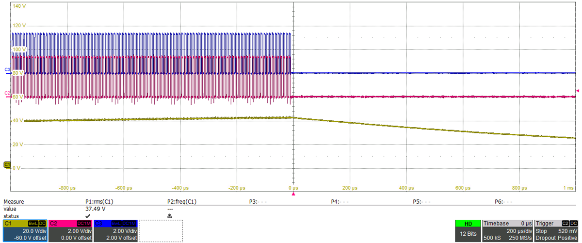 Figure 4-25 LAB 2 -
Overvoltage Protection
Figure 4-25 LAB 2 -
Overvoltage ProtectionThe previous waveforms show PWM is shut off by the comparator subsystem during fault events. The type of fault is displayed in the watch window through variable
DAB_tripFlag, see Figure 4-26. The trip can be reset by selecting noTrip under the drop-down menu and re-enabling the PWM by writing “1” to theDAB_clearTripvariable. Make sure the fault condition is removed before re-enabling the PWM.
- Primary overcurrent protection:
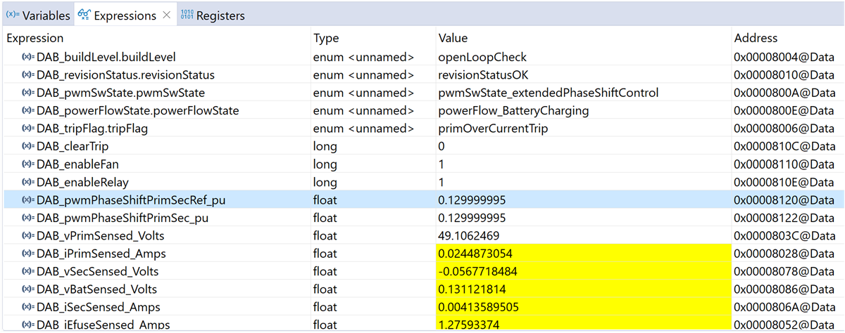 Figure 4-26 Trip Indication in Expression
Window
Figure 4-26 Trip Indication in Expression
Window- Measure SFRA Plant for Voltage
Loop
- The SFRA is integrated in the C2000Ware-DigitalPower-SDK kit to measure the plant response which can then be used to design a compensator. Run the SFRA by clicking on the SFRA icon. The SFRA GUI opens.
- Select the options for the device on the SFRA GUI; for example, for F280039, select floating point. Click the Setup Connection button. In the pop-up window, uncheck the boot-on-connect option and select an appropriate COM port. Select the OK button. Return to the SFRA GUI and click the Connect button.
- The SFRA GUI connects to
the device. A SFRA sweep can now be started by clicking the Start
Sweep button. The complete SFRA sweep takes a few minutes to
complete. Monitor the activity in the progress bar on the SFRA GUI or by
checking the flashing blue LED on the back of the control card, which
indicates UART activity.
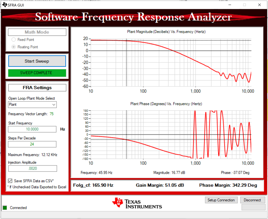 Test Condition: VIN = 800 V, VOUT = 500 V, IOUT = 10 A, phase shift = 0.047 pu.Figure 4-27 Lab 2 SFRA Plant Plot for the Open Voltage Loop Test
Noise in the phase plot is expected for higher frequencies due to noise in the output voltage measurement and small plant gain. - The Frequency Response
Data
SFRA.csvis saved in the project folder, under an SFRA Data Folder, and is time-stamped with the time of the SFRA run. SFRA can be run at different frequency setpoints to cover the range of operation of the system. A compensator is designed using these measured plots through compensator designer. Compensation designer can be opened from the main.syscfg GUI.Inside ISR1, the SFRA injects small signal perturbations in phase and observes the sensed output voltage variations. The following lines of code inside the dab.h file perform the SFRA signal injection and collection.
 Figure 4-28 Lab 2 Code for
SFRA Signal Injection
- Measure SFRA Plant for Current
Loop
- Follow the same steps as in voltage loop to get started with SFRA measurement for current loop.
- In the PowerSUITE GUI
under SFRA tab, choose current prior to running the SFRA current
loop.
 Figure 4-29 Lab 2 Code
Defines SFRA Current Loop
 - Inside ISR1, the SFRA
injects small signal perturbations in phase and observes the sensed
output current variations. The following lines of code inside the dab.h
file perform the SFRA signal injection and collection.
 Figure 4-30 Lab 2 Code for
SFRA Signal Injection
 - Measure the plant
response from SFRA GUI. The open loop and plant response are stored in
the file named
SFRA.csv. Use this file to tune the compensator for the current loop.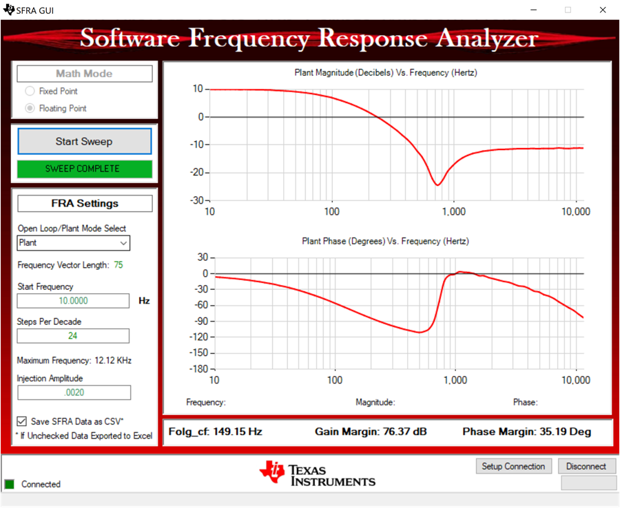 Test Condition: VIN = 800 V, VOUT = 500 V, IOUT = 10 A, phase shift = 0.047 puFigure 4-31 Lab 2 SFRA Plant Plot for the Open Current Loop Test