TIDUES0E June 2019 – April 2024 TMS320F28P550SJ , TMS320F28P559SJ-Q1
- 1
- Description
- Resources
- Features
- Applications
- 6
- 1System Description
- 2System Overview
- 3Circuit Description
- 4Hardware, Software, Testing Requirements, and Test Results
- 5Design Files
- 6Related Documentation
- 7Terminology
- 8About the Author
- 9Revision History
4.4.6 Lab 6
In this setup, the DC source is connected to the secondary side and the resistive load is connected to the primary side. The design is operated with closed-voltage loop in the reverse direction.
Compile the project by selecting 6: Closed Loop Voltage with Resistive Load, Sec to Prim Power Flow in the drop-down menu of Project Options from PowerSUITE GUI. Make sure current and voltage limits are set per operating conditions.
#if DAB_LAB == 6
#define DAB_CONTROL_RUNNING_ON C28X_CORE
#define DAB_POWER_FLOW DAB_POWER_FLOW_SEC_PRI
#define DAB_INCR_BUILD DAB_CLOSED_LOOP_BUILD
#define DAB_TEST_SETUP DAB_TEST_SETUP_RES_LOAD
#define DAB_PROTECTION DAB_PROTECTION_ENABLED
#define DAB_CONTROL_MODE  DAB_VOLTAGE_MODE
#define DAB_SFRA_TYPE  2
#define DAB_SFRA_AMPLITUDE (float32_t)DAB_SFRA_INJECTION_AMPLITUDE_LEVEL2
#endif- Test Setup for Lab 6 (Closed
Voltage Loop - Vprim - Reverse power flow)
- Run the project by clicking the green run button in CCS.
- Populate the required
variables in the watch window by loading JavaScript
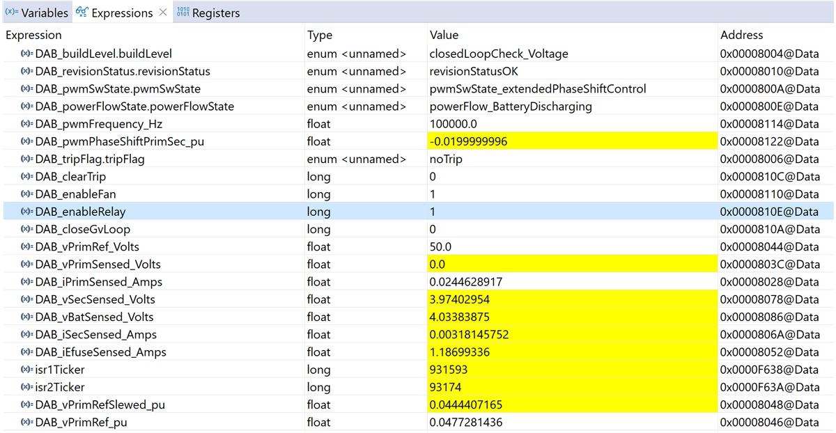
setupdebugenv_lab6.jsin the scripting console. Figure 4-46 Lab 6 - Watch
View
 - Enable fans and relays by
writing "1" into
DAB_enableFanandDAB_enableRelay. - Enable PWM by writing “1”
to the
DAB_clearTripvariable in the watch view. - Check if the
DAB_IprimSensed_Amps,DAB_iPrimSensed_Amps,DAB_vSecSensed_Volts, andDAB_iSecSensed_Ampsvariables are updating periodically. - Set the output voltage by
writing to
DAB_vPrimRef_Volts(in this example 50 Vdc). - Enable closed loop
operation by writing “1” to the
DAB_closeGvLoopvariable. The controller automatically adjusts the phase shift , depending upon the operating conditions to generate primary output voltage to match with that ofDAB_vPrimRef_Volts. - Now secondary side
voltage and
DAB_vPrimRef_Voltscan be increased in steps and the control behavior can be observed.
- Frequency response of closed
loop voltage
- Follow the same steps as
in Lab 3.
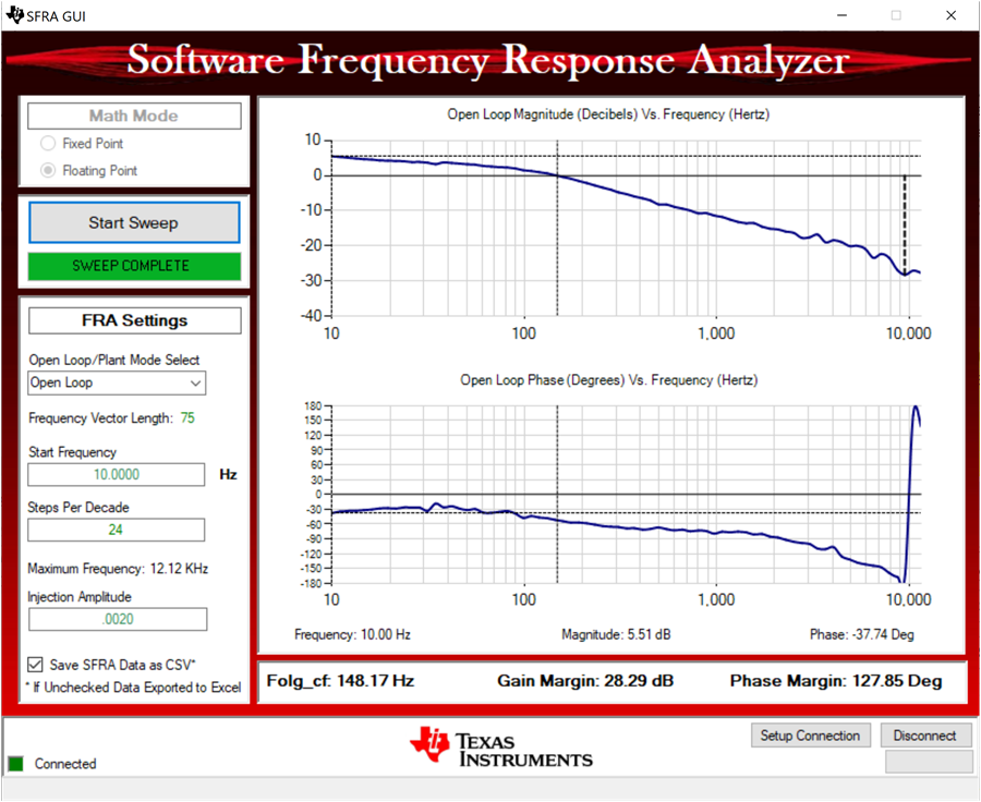
 Test Condition: VIN = 350 V, VOUT = 550 V, IOUT = 9 AFigure 4-47 Lab 6 - SFRA Open Loop Plot for the Closed Voltage Loop With Reverse Power Flow
VIN refers to secondary side voltage, VOUT and IOUT refer to primary side voltage and current in reverse direction. (DAB_IprimSensed_Amps = –9 A )The same controller and gains as in Lab 3 are used.
- Follow the same steps as
in Lab 3.