SCPS232B March 2012 – March 2016 PCA9515B
PRODUCTION DATA.
- 1 Features
- 2 Applications
- 3 Description
- 4 Revision History
- 5 Pin Configuration and Functions
- 6 Specifications
- 7 Parameter Measurement Information
- 8 Detailed Description
- 9 Application and Implementation
- 10Power Supply Recommendations
- 11Layout
- 12Device and Documentation Support
- 13Mechanical, Packaging, and Orderable Information
1 Features
- Two-Channel Bidirectional Buffers
- I2C Bus and SMBus Compatible
- Support for I2C Standard Mode (100-kHz) and Fast Mode (400-kHz)
- Active-High Repeater-Enable Input
- Open-Drain I2C Input and Output
- 5.5-V Tolerant I2C Input and Output and Enable Input Support Mixed-Mode Signal Operation
- Lockup-Free Operation
- Accommodates Standard Mode, Fast Mode I2C Devices, and Multiple Masters
- Supports Arbitration and Clock Stretching Across Repeater
- Powered-Off High-Impedance I2C Pins
- Latch-Up Performance Exceeds 100-mA Per JESD 78, Class I
- ESD Protection Exceeds JESD 22
- 2000-V Human-Body Model (A114-A)
- 1000-V Charged-Device Model (C101)
2 Applications
- Servers
- Routers (Telecom Switching Equipment)
- Industrial Equipment
- Products with Many I2C Slaves and Long PCB Traces
3 Description
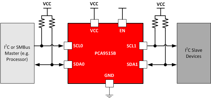
The PCA9515B is a BiCMOS dual bidirectional buffer integrated circuit intended for I2C bus and SMBus applications. The device contains two identical bidirectional open-drain buffer circuits that enables I2C and similar bus systems to be extended (or add slaves) without degrading system performance. The dual bidirectional I2C buffer is operational at 2.3 V to 3.6 V VCC.
The PCA9515B buffers both the serial data (SDA) and serial clock (SCL) signals on the I2C bus, while retaining all the operating modes and features of the I2C system. The device allows two buses, of 400-pF bus capacitance, to be connected in an I2C application.
Device Information(1)
| PART NUMBER | PACKAGE | BODY SIZE (NOM) |
|---|---|---|
| PCA9515B | VSSOP (8) | 3.00 mm × 3.00 mm |
- For all available packages, see the orderable addendum at the end of the data sheet.
Simplified Schematic
