SBAA338A March 2019 – June 2022 ADS7042 , ADS7142
| Input | ADC Input | Digital Output ADS7042 |
|---|---|---|
| VinMIn | 210 mV | 0x105 |
| VinMax | 3.09 V | 0xEFB |
| Power Supplies |
|---|
| AVDD |
| 3.3 V |
Design Description
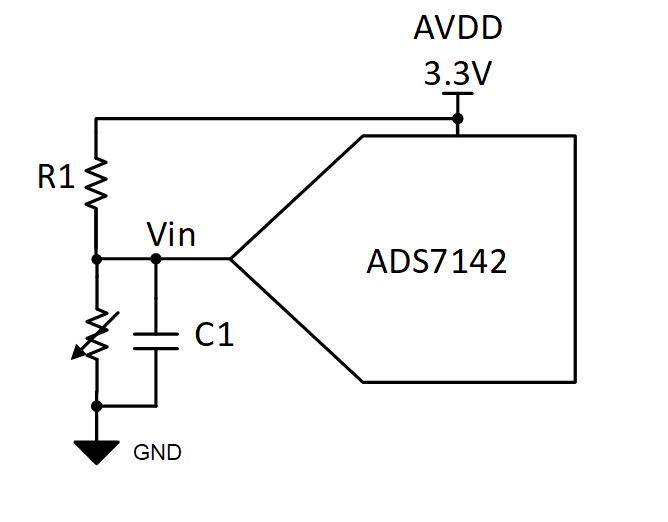
This document describes how to design a circuit to directly monitor temperature using a thermistor with a successive approximation register (SAR) analog-to-digital (ADC). This temperature sensing circuit monitors a temperature range from –25°C to 100°C using a negative temperature coefficient (NTC) thermistor in series with a resistor to form a voltage-divider. This voltage divider has the effect of producing an output voltage that is inversely related to the monitored temperature. The source voltage to the resister divider is the analog power supply (AVDD) to the analog to digital converter, ADS7142, which, for this device, is also the reference. By connecting the resistor divider to the reference input, AVDD, the measurements will be ratiometric which will ensure that variations in the reference voltage will not impact the overall accuracy. The capacitor in parallel with the input resistor is used to support ADC input settling performance.
Thermistors are used to monitor temperature in applications such as appliances, wireless environmental sensors, and smoke and heat detectors. In these applications, the thermistor voltage changes slowly thus it is not necessary to sample at high sampling rates. This means that there is no need for a driving input amplifier to condition the input voltage. A similar circuit design, Driving SAR directly without a front-end buffer circuit, explains how to measure introduced drift from external components which can prove to be helpful in these applications.
Specifications
| Specification | Calculated | Simulated |
|---|---|---|
Sampling Rate | < 10 kHz | 10 kHz, settling to ½ LSB |
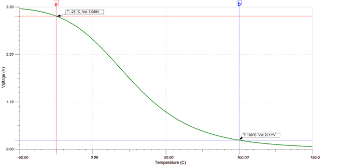
| Temperature range | –25°C to 100°C | –25°C to 100°C |
| ADC input range | 210 mV to 3.09 V | 212 mV to 3.09 V |
Design Notes
- Create a resistor divider topology with NTC thermistor as the second component of the resister divider. Using this configuration will cause the ADC input voltage to decrease with an increase in temperature. The input voltage will increase as the temperature decreases or the input voltage will decrease as the temperature increases.
- R1 in the resistor divider is designed based on the temperature range monitored. Use the thermistor resistance tolerance as a guideline for choosing the tolerance of R1. Typically, a 1% tolerance resistor is sufficient to match the thermistor tolerance, but a better performing resistor will be needed if stringent requirements are present. The equation used to calculate the value of R1 is provided in the following component section.
- The capacitor in parallel, C1 with the NTC is implemented to help support ADC input settling within the acquisition phase of the ADC sampling rate. The capacitor affects the start-up time of the system as it will take longer to charge larger capacitors.
Component Selection
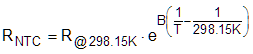
- Select a thermistor to best fit the application requirements needed. When selecting the thermistor, take into consideration the Beta value (B), a common parameter found in the device data sheet. The B value is specified across a given temperature range and represents the change of the resistance of the thermistor across that specified temperature range. The NTC selected in this example is a 100 kΩ at 25°C with a B(25/85) value of 3977.
- The expected extrema resistances the NTC will experience need to be calculated to select R1. The value of R1 will create a more linear voltage versus temperature relation. The following equation is used to find the NTC resistance based on temperature; calculations require temperature to be in Kelvin.
where
- RNTC is the thermistor resistance (Ω) at temperature T
- R@298.15K is the thermistor resistance (Ω) measured at 25°C given in the data sheet
- B is the thermistor B value from data sheet in Kelvin (K)
- T is the temperature in Kelvin (K) that the thermistor is at (0°C + 273.15 = K).
Temperature range in Kelvin:
- Tmin = –25°C + 273.15 = 248.15K
- Tmax = 100°C + 273.15 = 373.15K
Thermistor resistance values:
- Rmin = R@373.15K = 100kΩ ∙ e3977(1/373.15K - 1/248.15K) = 6.849 kΩ
- Rmax=R@248.15K = 100kΩ ∙ e3977(1/248.15K - 1/248.15K) = 1,469.744 kΩ
- Calculate the value of R1, using the expected minimum and maximum NTC resistances. The closest resister value is 100 kΩ.
R1 = √(R@373.15K ∙ R @248.15K) = √(6.849 kΩ ∙ 1,469.744 kΩ) = 100.333 kΩ
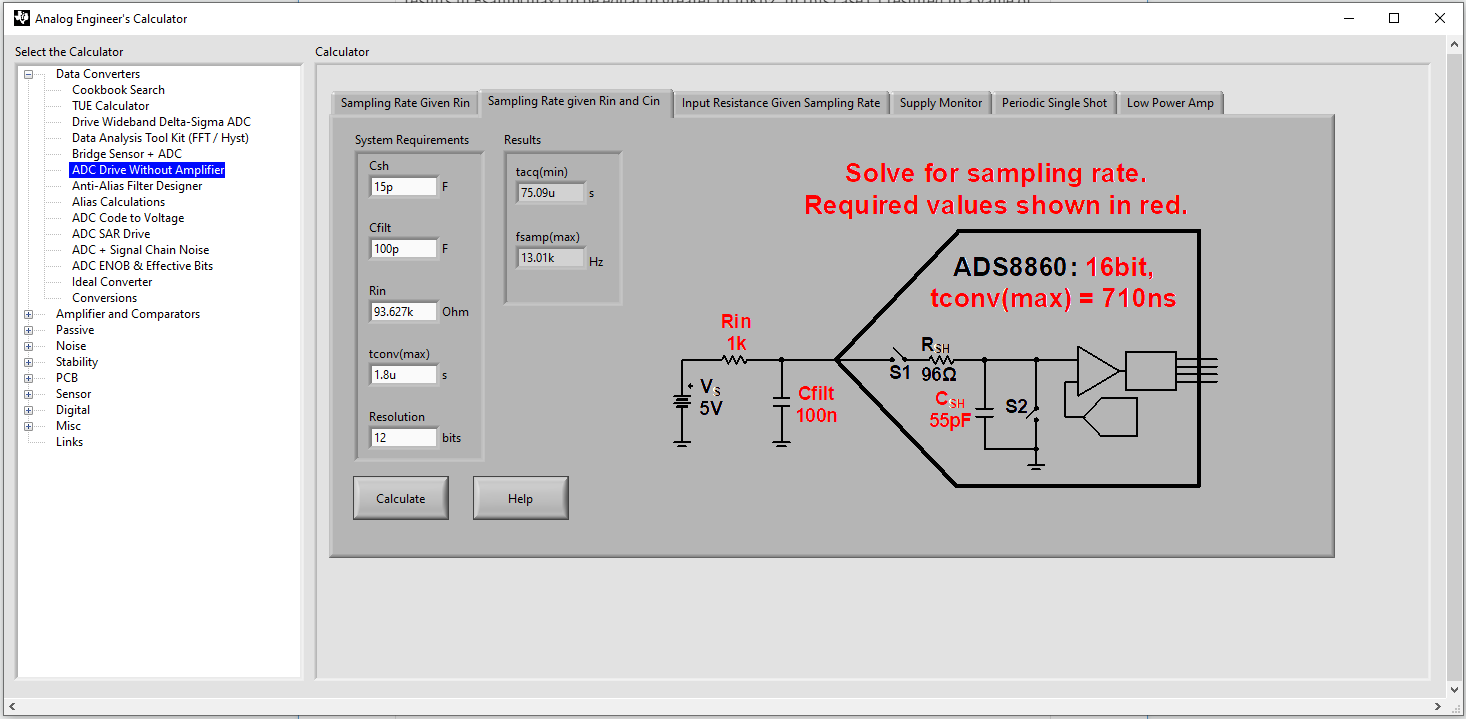
- Select the capacitor value. Base the capacitor value on the sampling rate the ADC will operate at since the capacitor functionality is to support ADC input settling performance. In this case the target sample rate is 10 kHz, with the max conversion time 1.8 μs.
Using the Analog Engineer Calculator can help design this value based on the operation of the system and values from the ADC data sheet. Within the calculator tool, select Data Converters > ADC Drive Without Amplifier, then select the Sampling Rate Given Rin and Cin tab. Use this tool to solve for C1 based on the calculated sampling rate achievable, Fsamp(max). Within this window, enter the ADC sample-and-hold capacitor, 15pF, the parallel equivalent of the resister divider at the worst-case settling scenario which is when the NTC is at the max resistive value, 93.627kΩ, the max conversion time, 1.8us, and the ADC resolution, 12. The initial Cfilt value entered should be 20 × the ADC sample-and-hold capacitor, in this case 15 pF ∙ 20 = 300 pF. Entering this value results in the maximum sample rate to be less the desired 10 kHz. From here, decrease Cfilt to a value that results in Fsamp(max) to be equal to or greater than 10 kHz. In this case, C1 resulted to a value of 100 pF.
- Run transient simulations to verify NTC performance across temperature and input settling within the acquisition time to be within half an LSB.
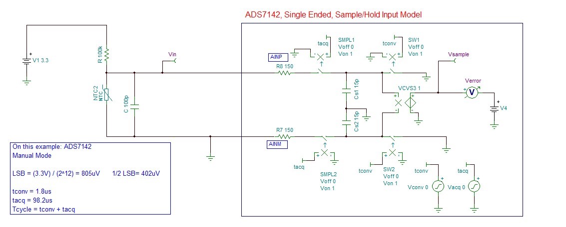
Design Simulation Model
The following schematic of the first order model of ADS7142 was built using the steps explained in TI Precision Labs –ADS: Building the SAR ADC model in TINA SPICE. The ADC sampling rate is set at 10 kHz.
Temperature Transfer Characteristics
The linear NTC voltage range for the desired temperature range of –25°C to 100°C is within the ADC input range and uses 87% of the ADC full scale range. The following equation is used to solve for the temperature measurement based on the resistor divider measured by the ADC. This does not include system calibration or system tolerances.
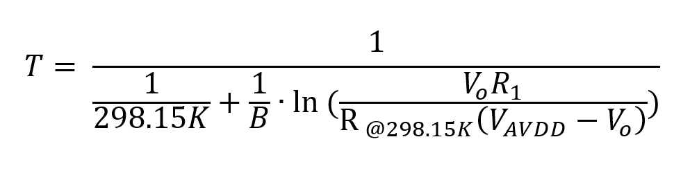
where:
- T is the temperature in Kelvin (K) (°C + 273.15 = K)
- Vo is the resistor divider output voltage measured by the ADC
- B is the thermistor B value of the NTC in Kelvin (K), in this case 3977
- R@298.15K is the thermistor resistance (Ω) at 25°C, in this case 100 kΩ
- VAVDD is the reference voltage and source voltage to the divider, in this case, 3.3 V
- R1 is 100 kΩ
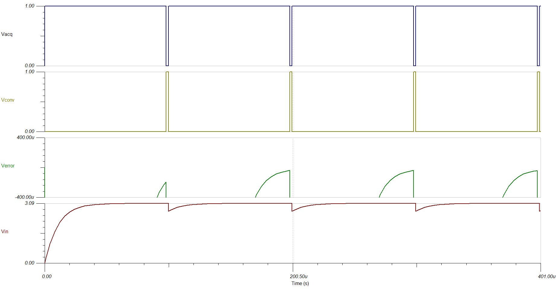
Transient DC Input Start-Up and Settling
Expected start-up time varies by the NTC resistance state. The following graph displays the maximum resistance value the NTC will experience, as this is the worst-case scenario for ADC input settling. The Verror graph shows that the input settling error is less than half of an LSB, ±402 μV, at the end of each acquisition period. See TI Precision Labs: Drive ADC Input for an explanation of ADC settling.
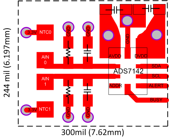
Small Layout
The ADS7142 is a dual-channel I2C ADC in a small X2QFN package size of 1.5 mm × 2 mm. The following image is a system-level solution using the ADS7142 with two NTCs connected at each analog input, though each input can monitor different types of sensors.
Design Featured Devices
| Device | Key Features | Link | Other Possible Devices |
|---|---|---|---|
| ADS7142(1) | 12-bit resolution, I2C, autonomous monitor, dual-channel single-ended input, small package size: 1.5 mm × 2 mm | ADS7142 | http://www.ti.com/adcs |
| ADS7042(1) | 12-bit resolution, SPI, 1MSPS sample rate, single-ended input, AVDD, Vref input range 1.6 V to 3.6 V | ADS7042 | http://www.ti.com/adcs |
Design References
See Analog Engineer's Circuit Cookbooks for TI's comprehensive circuit library.
Link to Key Simulation Files