SBAA501 May 2021 ADS124S06 , ADS124S08
Application Brief
Introduction
Whenever measuring temperature using a thermo couple (TC), it is necessary to also measure the temperature at the point where the TC connects to the board to get an accurate absolute reading. This cold junction compensation can be done with different types of temperature sensors, ranging from simple diodes over platinum thin film sensors up to digital temperature sensors. Digital sensors bring the benefit, that they are often factory calibrated. As they do not need an analog channel they can be added when running out of ADC channels or when there is a need for multiple sensors for the CJC. For more information about TC measurements and the CJC, see A Basic Guide to Thermocouple Measurements.
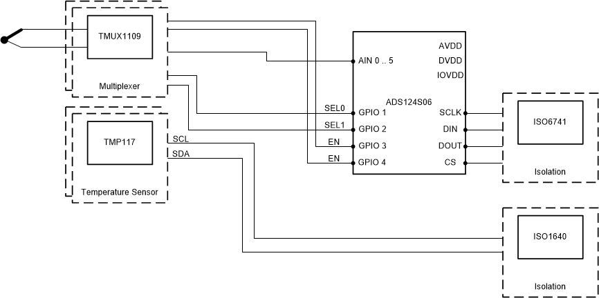
This document focuses on the use of digital sensors (for example, TMP117) with an I²C interface together with ADCs with integrated GPIOs (for example, ADS124S06) and SPI. Figure 1-1 shows how a typical system approach could be implemented.

Figure 1-1 CJC With I²C Sensor and Isolation
The ADC ADS124S06 is the main part in this system; using two multiplexers, the number of available input channels of the ADC gets extended. The multiplexers can be controlled using the GPIO lines.
For the cold-junction compensation, a couple of temperature sensors TMP117 with I2C interface are added. Since TC systems often need to be isolated to avoid ground loops, an isolator for the SPI lines of the ADC ISO6741 and an isolator for I²C ISO1640 are added.
An MCU now has to be connected on the other side of the isolation barrier to the SPI and I²C interface. The SPI and I²C can be handled independently from each other and in high speed. The multiplexer channels can be switched from the MCU through SPI connection and the GPIOs of the ADC.
Using GPIOs for I²C
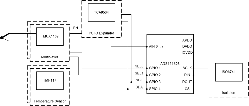
To simplify this design and remove the I²C isolator, as well as the need of an additional I²C interface on the MCU, the GPIOs of the ADC can be used for bit banging an I²C interface.
Figure 1-2 shows the modified block diagram. Two of the GPIO lines are now used as an I²C interface that connects to the TMP117 and to control the enable lines of the multiplexers an additional IO expander is added.

Figure 1-2 I2C Over Isolated SPI
As this is a bit banged I²C interface, it is much slower than a hardware peripheral. The fact that it has to be transmitted from the MCU to the ADC through SPI also limits the speed.

Figure 1-3 I2C and SPI Communication
When looking at the SPI and I²C communication in parallel, as shown in Figure 1-3, it is clearly visible, that a lot of communication is necessary on the SPI for a rather slow I²C. Nevertheless, here the SPI clock is set to 2 MHz and a TMP117 can be read in about 4.5 ms. Increasing the SPI clock rate would also increase the I²C clock rate and so reduce the time needed for reading a temperature sample.
Even though the speed is rather low, it is still fast enough for taking temperature readings. The switching from the I²C communication can influence the ADC reading and increase the noise. To keep this effect low, the user can start communicating right after starting the conversion. To remove effects completely it is recommended to not have a conversion running in parallel, or to discard the reading that was captured in parallel.
Adding More Temperature Sensors
In many cases one temperature sensor will not be enough. As each device on an I²C bus must have a unique address, the address of the TMP117 can be configured. The address pin allows up to four different addresses, as Table 1-1 shows.
| Device Address | ADD0 Pin Connection |
|---|---|
| 1001000x | GND |
| 1001001x | V+ |
| 1001010x | SDA |
| 1001011x | SCL |
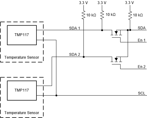
If even more sensors are needed on one I²C bus, it is necessary to switch the SDA line of each group of devices.
Figure 1-4 shows how to use a few discrete components to switch between different I²C devices with the same address. One MOSFET is used to turn on or off the corresponding SDA line. Remember from the complete circuit the enable signal can come from the IO expander, for example. This allows addition of up to eight TMP117 temperature sensors to one I²C bus.

Figure 1-4 Multiplexing I2C
A closer examination of the SDA1 signal shows that the switched SDA signal still has voltage levels that are in the valid range. Compared to before, the SPI clock is now increased to the maximum allowed SPI clock for the ADS124S06 of 10 MHz – and with this – the I²C frequency in this example is at 20 kHz, which allows to read a temperature reading in less than 2 ms.

Figure 1-5 Reading TMP117
Summary
This application brief shows how to interface an I²C temperature sensor such as TMP117 or TMP116 through the GPIOs of an ADC. This allows use of only one SPI isolator for implementing an isolated SPI and I²C communication. The methodology for adding multiple I²C devices to one bus, even when addresses are duplicated is also provided.
References and Related Parts
- Texas Instruments, ADS124S0x Low-Power, Low-Noise, Highly Integrated, 6- and 12-Channel, 4-kSPS, 24-Bit, Delta-Sigma ADC with PGA and Voltage Reference Data Sheet
- Texas Instruments, TMP117 High-Accuracy, Low-Power, Digital Temperature Sensor Data Sheet
- Texas Instruments, TMP116 High-Accuracy, Low-Power, Digital Temperature Sensor Data Sheet
- Texas Instruments, A Basic Guide to Thermocouple Measurements Application Report