SBASAG2C December   2023  – March 2025 ADS9227 , ADS9228 , ADS9229

PRODUCTION DATA  

  1.   1
  2. 1 Features
  3. 2 Applications
  4. 3 Description
  5. 4 Device Comparison Table
  6. 5 Pin Configuration and Functions
  7. 6 Specifications
    1. 6.1  Absolute Maximum Ratings
    2. 6.2  ESD Ratings
    3. 6.3  Thermal Information
    4. 6.4  Recommended Operating Conditions
    5. 6.5  Electrical Characteristics
    6. 6.6  Timing Requirements
    7. 6.7  Switching Characteristics
    8. 6.8  Timing Diagrams
    9. 6.9  Typical Characteristics: All Devices
    10. 6.10 Typical Characteristics: ADS9229
    11. 6.11 Typical Characteristics: ADS9228
    12. 6.12 Typical Characteristics: ADS9227
  8. 7 Detailed Description
    1. 7.1 Overview
    2. 7.2 Functional Block Diagram
    3. 7.3 Feature Description
      1. 7.3.1  Analog Inputs
      2. 7.3.2  Analog Input Bandwidth
      3. 7.3.3  ADC Transfer Function
      4. 7.3.4  Reference
        1. 7.3.4.1 Internal Reference Voltage
        2. 7.3.4.2 External Reference Voltage
      5. 7.3.5  Temperature Sensor
      6. 7.3.6  Data Averaging
      7. 7.3.7  Digital Down Converter
      8. 7.3.8  Data Interface
        1. 7.3.8.1 Data Frame Width
        2. 7.3.8.2 ADC Output Data Randomizer
        3. 7.3.8.3 Synchronizing Multiple ADCs
      9. 7.3.9  Test Patterns for Data Interface
        1. 7.3.9.1 Fixed Pattern
        2. 7.3.9.2 Digital Ramp
        3. 7.3.9.3 Alternating Test Pattern
      10. 7.3.10 ADC Sampling Clock Input
    4. 7.4 Device Functional Modes
      1. 7.4.1 Reset
      2. 7.4.2 Power-Down Options
      3. 7.4.3 Normal Operation
      4. 7.4.4 Initialization Sequence
    5. 7.5 Programming
      1. 7.5.1 Register Write
      2. 7.5.2 Register Read
      3. 7.5.3 Multiple Devices: Daisy-Chain Topology for SPI Configuration
        1. 7.5.3.1 Register Write With Daisy-Chain
        2. 7.5.3.2 Register Read With Daisy-Chain
  9. 8 Register Map
    1. 8.1 Register Bank 0
    2. 8.2 Register Bank 1
    3. 8.3 Register Bank 2
  10. 9 Application and Implementation
    1. 9.1 Application Information
    2. 9.2 Typical Applications
      1. 9.2.1 Data Acquisition (DAQ) Circuit for ≤20kHz Input Signal Bandwidth
        1. 9.2.1.1 Design Requirements
        2. 9.2.1.2 Detailed Design Procedure
        3. 9.2.1.3 Application Curves
      2. 9.2.2 Data Acquisition (DAQ) Circuit for ≤100kHz Input Signal Bandwidth
        1. 9.2.2.1 Design Requirements
        2. 9.2.2.2 Application Curves
      3. 9.2.3 Data Acquisition (DAQ) Circuit for ≤1MHz Input Signal Bandwidth
        1. 9.2.3.1 Design Requirements
        2. 9.2.3.2 Application Curves
    3. 9.3 Power Supply Recommendations
    4. 9.4 Layout
      1. 9.4.1 Layout Guidelines
      2. 9.4.2 Layout Example
  11. 10Device and Documentation Support
    1. 10.1 Documentation Support
      1. 10.1.1 Related Documentation
    2. 10.2 Receiving Notification of Documentation Updates
    3. 10.3 Support Resources
    4. 10.4 Trademarks
    5. 10.5 Electrostatic Discharge Caution
    6. 10.6 Glossary
  12. 11Revision History
  13. 12Mechanical, Packaging, and Orderable Information

Register Write

Register write access is enabled by setting SPI_RD_EN = 0b. The 16-bit configuration registers are grouped in three register banks and are addressable with an 8-bit register address. Register bank 1 and register bank 2 are selected for read or write operation by configuring the REG_BANK_SEL bits. Registers in bank 0 are always accessible, irrespective of the REG_BANK_SEL bits. The register addresses in bank 0 are unique and are not used in register banks 1 and 2.

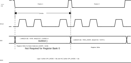
As shown in Figure 7-13, steps to write to a register are:

  1. Frame 1: Write to register address 0x03 in register bank 0 to select either register bank 1 or bank 2 for a subsequent register write. This frame has no effect when writing to registers in bank 0.
  2. Frame 2: Write to a register in the bank selected in frame 1. Repeat this step for writing to multiple registers in the same register bank.
ADS9227 ADS9228 ADS9229 Register Write Figure 7-13 Register Write