SBAU374A May 2021 – May 2022 DAC12DL3200
- Abstract
- Trademarks
- 1Introduction
- 2Equipment
-
3Setup Procedure
- 3.1 Install the High Speed Data Converter (HSDC) Pro Software
- 3.2 Install the Configuration GUI Software
- 3.3 Connect the DAC12DL3200EVM and TSW14DL3200EVM
- 3.4 Connect the Power Supplies to the Boards (Power Off)
- 3.5 Connect the Signal Generators to the EVM (*RF Outputs Disabled Until Directed)
- 3.6 Turn On the TSW14DL3200EVM 12-V Power and Connect to the PC
- 3.7 Turn On the DAC12DL3200EVM 5-V Power Supply and Connect to the PC
- 3.8 Turn On the Signal Generator RF Outputs
- 3.9 Open the DAC12DL3200EVM GUI and Program the DAC and Clocks for Single Channel, NRZ Mode 2 Operation
- 3.10 Open the HSDC Software and Load the FPGA Image to the TSW14DL3200EVM
- 3.11 DxSTRB Timing Adjustment
- 4Other Modes of Operation
- 5Register Log File
- 6Device Configuration
- A Troubleshooting the DAC12DL3200EVM
- B DAC12DL3200EVM Onboard Clocking Configuration
3.11 DxSTRB Timing Adjustment
- By default, the current firmware used by HSDC Pro
sends a square wave instead of a pulse for the DxSTR signals. The DAC requires a
pulse for DxSTR that needs to be a width that is a multiple of 4 LVDS clock
cycles. To correct for this, do the following in HSDC Pro GUI:
- Click on the Instrument Options tab located in the top left of the DAC main page.
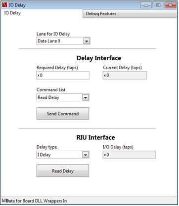
- Click on IO
Delay.
 Figure 3-8 IO
Delay
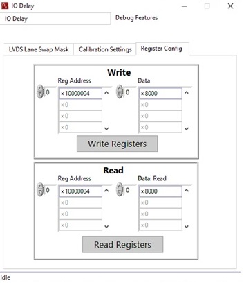
 - Click the Debug Features button.
- Enter x10000004 for the
Reg Address and x8000 for the Data in the Write section as shown in
Figure 3-9.
Click the Write Registers button. Enter x10000004 for the
RegAddress in the Read section. Click the Read Registers button.
Verify x8000 was written to this address. Close this window.
 Figure 3-9 IO Delay
Register WriteNote: These steps only need to be done once after the firmware has been loaded. If you send another pattern, you do not have to do these steps. If the TSWS14DL3200EVM is powered down or firmware is reloaded, these steps must be repeated.
 - In the HSDC Pro GUI main page, click the Send button in the upper left to send the test tone to the DAC EVM.
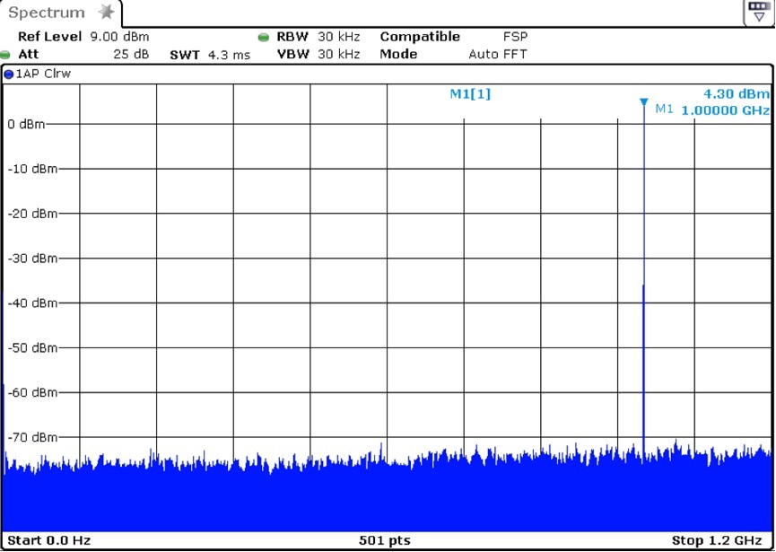
- There should now be a 1-GHz output tone on CHA SMA connector J1.
 Figure 3-10 DAC Channel A Output