SBAU374A May 2021 – May 2022 DAC12DL3200
- Abstract
- Trademarks
- 1Introduction
- 2Equipment
-
3Setup Procedure
- 3.1 Install the High Speed Data Converter (HSDC) Pro Software
- 3.2 Install the Configuration GUI Software
- 3.3 Connect the DAC12DL3200EVM and TSW14DL3200EVM
- 3.4 Connect the Power Supplies to the Boards (Power Off)
- 3.5 Connect the Signal Generators to the EVM (*RF Outputs Disabled Until Directed)
- 3.6 Turn On the TSW14DL3200EVM 12-V Power and Connect to the PC
- 3.7 Turn On the DAC12DL3200EVM 5-V Power Supply and Connect to the PC
- 3.8 Turn On the Signal Generator RF Outputs
- 3.9 Open the DAC12DL3200EVM GUI and Program the DAC and Clocks for Single Channel, NRZ Mode 2 Operation
- 3.10 Open the HSDC Software and Load the FPGA Image to the TSW14DL3200EVM
- 3.11 DxSTRB Timing Adjustment
- 4Other Modes of Operation
- 5Register Log File
- 6Device Configuration
- A Troubleshooting the DAC12DL3200EVM
- B DAC12DL3200EVM Onboard Clocking Configuration
6.2 Low-Level Control
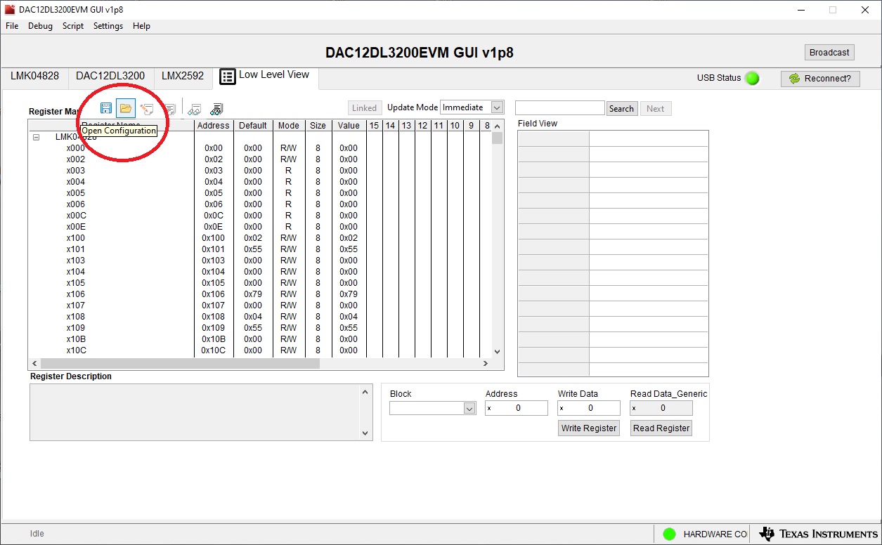
The Low Level View tab illustrated in Figure 6-1, allows configuration of the devices at the bit-field level. At any time, use the controls in Table 6-1 to configure or read from the device.
 Figure 6-1 Configuration GUI: Low-Level View Tab
Table 6-1 Low-Level Controls
| Control | Description |
|---|---|
| Register map summary | Displays the devices on the EVM, registers
for those devices, and the states of the registers
|
| Write register button | Write to the register highlighted in the register map summary with the value in the Write Data field |
| Write all button | Update all registers shown in the register map summary with the values shown in the Register Map summary |
| Read register button | Read from the register highlighted in the
Register Map summary and display the
results in the Read Data field Can be used to synchronize the GUI with the state of the hardware |
| Read-all button | Read from all registers in the Register Map summary and display the current state of the hardware |
| Load Configuration button | Load a configuration file from disk and register address/data values in the file |
| Save Configuration button | Save a configuration file to disk that contains the current state of the configuration registers |
| Register Data cluster | Manipulate individual accessible bits of the register highlighted in the register map summary |
| Individual register cluster with read or write register buttons | Perform a generic read or write command to the device shown in the Block drop-down menu using the address and write data information |