SBAU383A June 2021 – February 2022 BUF802
8 Schematic
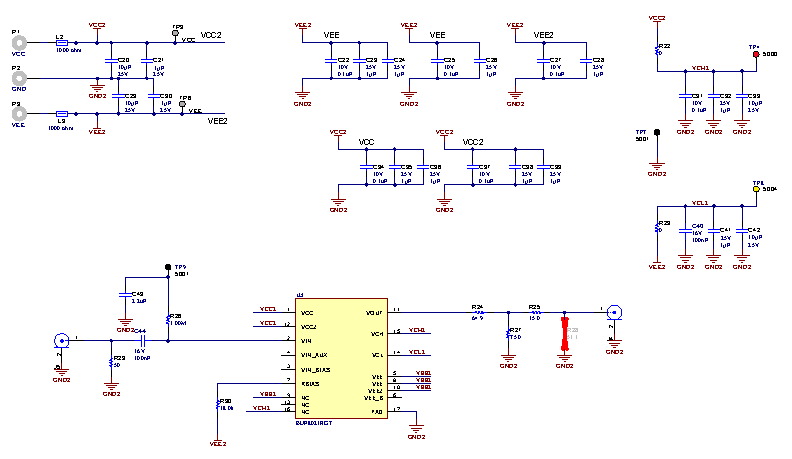
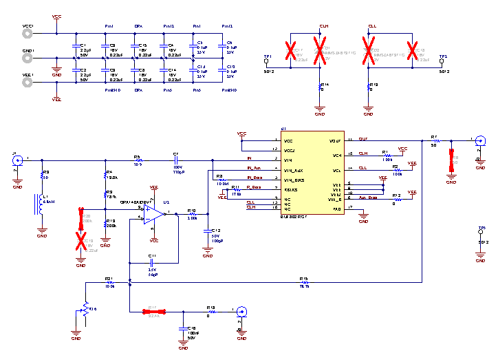
Figure 8-1 and Figure 8-2 show the BUF802RGTEVM schematic with the default device population for both circuits.
 Figure 8-1 BUF802RGTEVM Standalone Configuration Schematic
 Figure 8-2 BUF802RGTEVM Composite Configuration Schematic