SBOA332A January 2019 – September 2024 THS4131 , THS4535 , THS4561
Design Goals
| Input | Output | Supply | |
|---|---|---|---|
| Single-Ended | Differential | Vcc | Vee |
| 0V to 1V | 16Vpp | 10V | 0V |
| Output Common-Mode | 3 dB Bandwidth | AC Gain (Gac) |
|---|---|---|
| 5V | 3MHz | 16V/V |
Design Description
This design uses a fully-differential amplifier (FDA) as a single-ended input to differential output amplifier.

Design Notes
- The ratio R4/R3, equal to R2/(R5||R6), sets the gain of the amplifier.
- The main difference between a single-ended input and a differential input is that the available input swing is only half. This is because one of the input voltages is fixed at a reference.
- It is recommended to set this reference to mid-input signal range, rather than the min-input, to induce polarity reversal in the measured differential input. This preserves the ability of the outputs to crossover, which provides the doubling of output swing possible with an FDA.
- The impedance of the reference voltage must be equal to the signal input resistor. This can be done by creating a resistor divider with a Thevnin equivalent of the correct reference voltage and impedance.
Design Steps
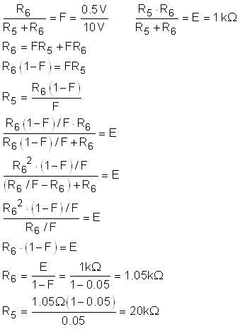
- Find the resistor divider with that produces a 0.5V, 1-kΩ reference
from Vs = 10V.
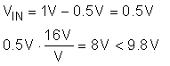
- Verify that the minimum input of 0V and the maximum input of 1V
result in an output within the 9.4V range available for Vocm = 5V.
Since the resistor divider acts like a 0.5V reference, the measured differential input for a 0V VIN is:

- The output is:

- Likewise, for a 1 V input:
Note:
With a reference voltage of 0V, a 1V input results in an output voltage greater than the maximum output range of the amplifier.
Design Simulations
 AC Simulation Results
 Transient Simulation Results
Design References
Texas Instruments, Design a front-end to drive a differential ADC, Precision labs video
Design Featured Op Amp
| THS4561 | |
|---|---|
| Vss | 3V to 13.5V |
| VinCM | Vee-0.1V to Vcc-1.1V |
| Vout | Vee+0.2V to Vcc-0.2 |
| Vos | TBD |
| Iq | TBD |
| Ib | TBD |
| UGBW | 70MHz |
| SR | 4.4V/µs |
| #Channels | 1 |
| THS4561 | |
Design Alternate Op Amp
| THS4131 | |
|---|---|
| Vss | 5V to 33V |
| VinCM | Vee+1.3V to Vcc-0.1V |
| Vout | Varies |
| Vos | 2mV |
| Iq | 14mA |
| Ib | 2µA |
| UGBW | 80MHz |
| SR | 52V/µs |
| #Channels | 1 |
| THS4131 | |