SBOA343A March 2019 – March 2022 INA180-Q1 , INA181-Q1 , INA186-Q1 , INA240-Q1
1
Monitoring current off an automotive 12-V battery provides critical data for a variety of applications such as module current consumption, load diagnostics, and load feedback control. The TI current sensing portfolio can address this space with analog and digital current sense amplifier (CSA) devices that come automotive qualified, contain integrated features, and operate in 12-V environments even though powered with low-voltage rails. This document provides recommended devices and architectures to address current sensing in this space.
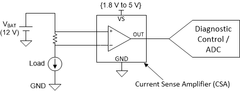
 Figure 1-1 Current Sense Amplifier on
12-V Rail
Figure 1-1 Current Sense Amplifier on
12-V RailThere are constraints in this space that stem from conditions such as electrical transient protection regulations ISO7637-2 and ISO16750-2, jump-starts, reverse-polarity, and cold-cranking. In general, system-level protection and suppression schemes can be used to protect downstream circuitry from these voltage surge conditions. Types of devices included in these solutions are smart high-side switches, smart diodes, or other discrete implementations. These products may come with internal integrated current sensing features, but they often are not very accurate (±3% to ±20% maximum error) and have limited dynamic range.
Dedicated TI current sensors are low in power consumption and highly accurate (<1% error) in automotive environments even across temperature.
A matched internal gain network plus input offset zeroing provides lower measurement drift across temperature compared to either discrete solutions or ICs with supplemental integrated current sensing. This amplifier integration and technology can remove the need for temperature and system calibrations, all at low cost.
Usually, general system protection schemes do not fully suppress or protect against voltage surges, so these primary regulations translate into typical voltage survivability requirements. Depending on the system, a current sensor may need to survive load dumps, reverse battery protection, fast load-switching, and inductive kickback voltages. For example, working on a 12-V battery rail requires at least 40-V survivability during load dump conditions. It is important to choose a current sensor that has an input common-mode voltage (VCM) rating that complies with the worst-case VCM condition of the system. Otherwise, input voltage clamping schemes are needed to protect the device during such conditions.
There are multiple TI Current (Power) Sensing amplifiers that can operate on a 12-V automotive battery and survive crucial voltage levels up to 40 V and more. Ultimately, they provide very accurate, zero-drift, high bandwidth, and low-cost solutions. Using TI's Product selection tool online, Table 1-1 tabulates candidates for high-side current sensing on an automotive 12-V battery rail requiring 40-V survivability. It should be noted that all devices in Table 1-1 have multiple gain variants ranging from 20 V/V to 500 V/V.
| TI Current Sense Amplifier |
VCM
Survivability |
VOS_MAX (25 °C) |
BW | Gain Error MAX (25 °C) | IQ_MAX (25 °C) |
Features |
|---|---|---|---|---|---|---|
| INA240-Q1 | -6 V to +90 V | ±25 µV | 400 kHz | ±0.2% | 2.4 mA | PWM rejection (very high CMRR), AEC Q100 (temperature grades 1 and 0) |
| INA190-Q1 | -0.3 V to +42 V | ±10 µV | 45 kHz | ±0.3% | 65 µA | More accurate version of INA186-Q1. Wide dynamic range. |
| INA186-Q1 | -0.3 V to +42 V | ±50 µV | 45 kHz | ±1% | 65 µA | Low input bias current (IB = ±500 pA typical). Wide dynamic range. Operates with supply voltage (VS) of 1.7 V. |
| INA180-Q1 (INA181-Q1) | -0.3 V to +28 V | ±500 µV | 350 kHz | ±1% | 0.5 mA | Single, dual, and quad channel. Uni- or bi-directional versions |
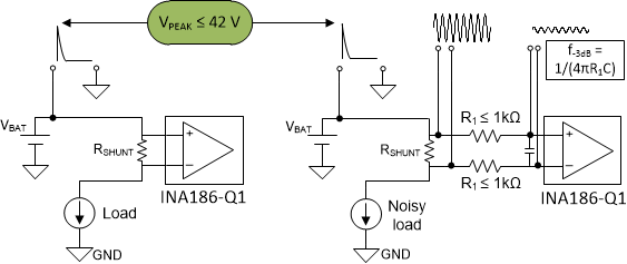
According to Table 1-1, the INA240-Q1 provides the best performance, but is not optimized to monitor a 12-V battery compared to INA186-Q1, which requires less power, cost, and package size. The INA186-Q1 does have high AC CMRR (140 dB) and large dynamic range (VOUT swings to VS - 40 mV over temperature). Additionally, the INA186-Q1 possesses a unique capacitively-coupled input architecture that increases differential input-resistance by 3 orders of magnitude compared to majority of CSAs. High input-impedance allows the user to filter current noise at the device input with minimal effect on gain. Using the data sheet equation if R1 = 1 kΩ, the effective gain is reduced 43.5 m% for all variants except A1 (25 V/V). Figure 1-2 shows use of INA186-Q1 in battery monitoring. Filtering at the input (instead of output) means current noise is not amplified and the INA186-Q1 can drive a cleaner signal into the ADC without an output filter loading down the ADC.
 Figure 1-2 INA186-Q1 On 12-V Battery With
and Without Noise Filtering
Figure 1-2 INA186-Q1 On 12-V Battery With
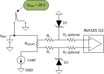
and Without Noise FilteringThe breadth of the current sense portfolio enables the user to optimize tradeoffs when incorporating common input protection schemes. If the chosen device states that the Absolute Maximum Common-Mode Voltage rating cannot exceed your maximum expected voltage surge, then it needs input protection. Along with some passives, the current sensor needs transient voltage suppression (TVS) or Zener diodes at the inputs for protection. Figure 1-3 shows an example using the cost-optimized current sensor INA181-Q1.
 Figure 1-3 INA181-Q1 with Input
Protection for VCM > 28 V
Figure 1-3 INA181-Q1 with Input
Protection for VCM > 28 VIn Figure 1-3, diodes D1 clamp the input VCM of the device to less than 28 V, which is the absolute maximum for INA181-Q1. R2 is optional and can be included to prevent simultaneous turn-on for D1 and the internal ESD structure of the CSA, but it is usually not needed. If it is needed, R2 should be small compared to R1. The power rating of diodes depends on the maximum expected voltage rise, but more importantly on the turn-on current. The diode current can be reduced by increasing R1 resistance, but this reduces the effective gain of the circuit and, more critically, increases gain error variation for most current sensors (except INA186-Q1).
Given the internal resistor gain network and input differential resistance of the INA181-Q1, an engineer can calculate the effective circuit gain with R1 using the equation in the data sheet. Keep in mind that adding external resistors broaden the system gain error variance beyond the data sheet limits. This is due to the fact that INA181-Q1 internal resistors are matched to be ratio metric, but are not trimmed to their typical values, so their absolute values can vary by ±20%.
Overall, an engineer can choose the INA181-Q1 because total cost with input protection is lower and increase in gain error variation is acceptable; however, devices with higher rated VCM are more straightforward solutions that provide accurate current sensing over temperature with less complexity and fewer components.
Alternate Device Recommendations
See Table 1-2 for applications that need either larger VCM ranges or integrated features such as shunt resistors or comparators.
| Device | Optimized Parameters | Performance Tradeoff |
|---|---|---|
| INA253 | Integrated 2 mΩ shunt resistor (included in Gain Error spec). Enhanced PWM rejection | IQ |
| INA301-Q1 | BW and slew rate. Internal comparator with adjustable threshold and 1 µs alert response time | 40 V VCM max |
| INA302-Q1, INA303-Q1 | BW and slew rate. Dual comparator output with adjustable thresholds and 1 µs alert response time | 40 V VCM max |
| LMP8278Q-Q1 | -12 V to +50 V VCM survivability. Adjustable gain and filtering. Buffered output | VOS |
| INA1x8-Q1, INA1x9-Q1 | ≥60 VCM. Current output (adjustable gain). Trimmed input resistors. Low IB when powered off | VOS |