SBOA502 December 2020 OPA462
2 Bridged Output Piezoelectric Actuator Driver
Consider an example case where the target voltage
range of a hypothetical actuator extends from –30 V to
+170 V. While this is a relatively “low voltage” in the field of piezo actuators, it
still requires a “high-voltage” op amp circuit to drive it. The OPA462 precision op
amp can use an 180-V supply, but on its own would still be unable to drive this
particular actuator to its maximum expansion. However, by employing an additional lower
voltage
(36 V) op amp such as the OPA192 along with
the OPA462 in a “bridge” configuration, the full 200 V needed for full actuator
response can be achieved. In the bridged output design the OPA462 (U1) serves
as the “high side” driver, while the OPA192 (U2) serves
as the “low side” driver.
We can determine the supplies needed to power the OPA462 and OPA192 as follows:
High piezo voltage = (VCC1 – U1 output swing to positive rail) – (VEE2 – U2 output swing to negative rail)
170 V = (VCC1 – 3 V) – (VEE2 – –1 V) → VCC1 – VEE2 = 174 V
Low piezo voltage = (VEE1 – U1 output swing to negative rail) – (VCC2 – U2 output swing to positive rail)
–30 V = (VEE1 – –5 V) – (VCC2 – 1 V) → VEE1 – VCC2 = –36 V
Observe that output voltage of U2 (VF2) does not actually need to swing –36 V below ground. VF2 simply needs to be 180° out of phase relative to the output voltage of U1 (VF1). It is the reversal of the maximum output voltages of U1 and U2 that result in the maximum voltage of 200 V being applied to the actuator. Simply stated, VF1 – VF2 = 170 V – (–30 V) = 200 V. Since both U1 and U2 are driven by the same input voltage source, different DC biases and gains are required for each amplifier. This is accomplished by establishing a unique DC input voltage at each non-inverting input, and setting the closed-loop gain of each op amp to the appropriate level.
The next step is actually selecting the supply rail voltages. To do this, first consider the input common-mode range of the two op amps. The OPA192 can accommodate a common-mode input as low as –100 mV below the VEE2. However, for the OPA462 this value cannot be lower than +1 V above the VEE1. The negative supplies VEE1 and VEE2 are set to –1 V to reduce the number of supply voltages needed. That allows the minimum common-mode input voltage applied at U1 to be 0 V. Although a –1-V supply is not common, –1.2 V can be easily provided from a linear, low-dropout regulator such as the TI TPS723, which accepts a –2.7 to –10 V input. For the positive supply, VCC1 should be at least 173 V. It can be as high as 179 V, and 175 V is selected for simplicity. VCC2 will be set to 35 V. If the VCC supply voltages differ by a few volts from +175 V and +35 V, then the resistor circuits used to set the voltage at the non-inverting inputs of U1 and U2 will need to be adjusted to maintain the correct bias levels.
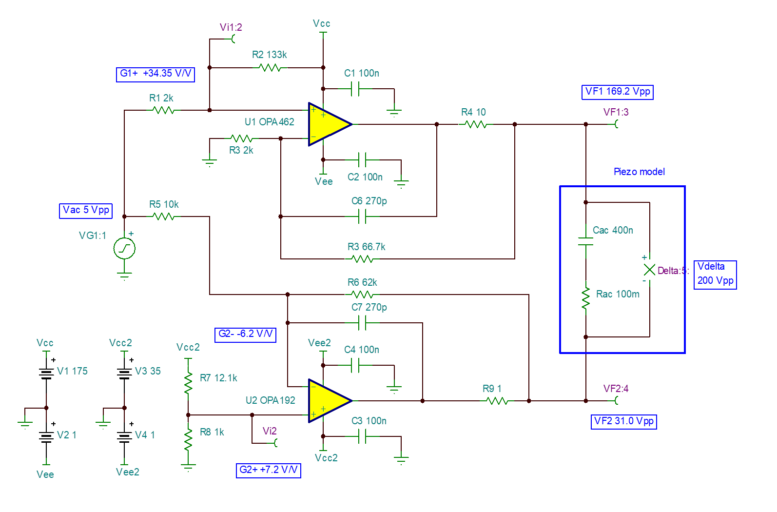
Figure 2-1 shows a TINA-TI
schematic for the bridged output piezo driver. The piezo load is modeled as a
400-nF capacitor, with 100 mΩ of series resistance to
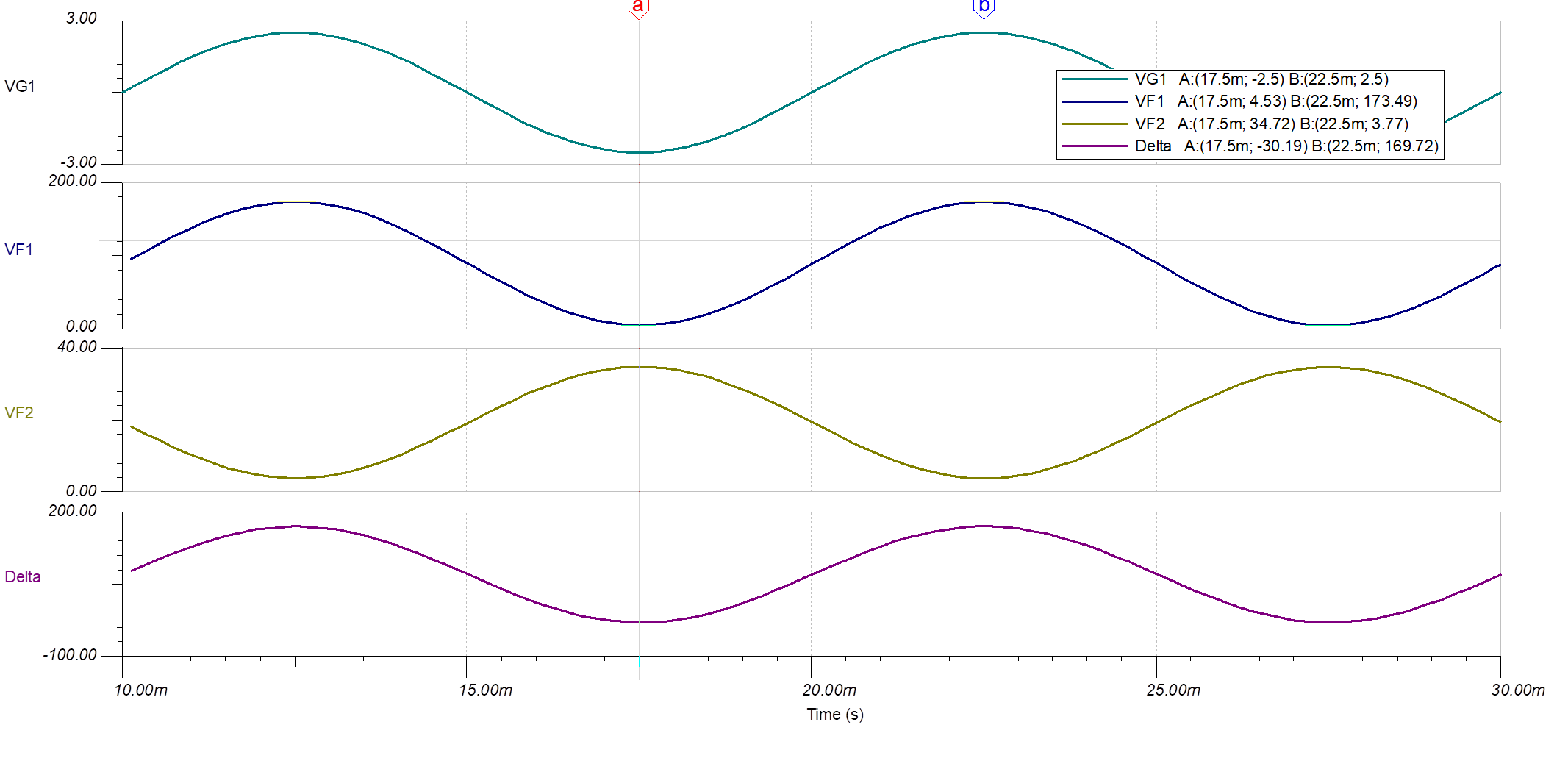
model the loss component. Figure 2-2 shows the results of
a transient simulation of the system when source VG1 is a 5 Vpp, 100-Hz sinusoidal
waveform. The system is compensated using a dual feedback, resistive isolation technique
(RISO) to maintain stability even with the very high 400-nF load. The op
amp drive currents peak at about ±25 mA, which both the OPA462 and OPA192 can provide. The bias voltage at the U1 non-inverting input (labeled
as Vi1 in Figure 2-1) is +2.59 Vdc. The
corresponding voltage Vi2 at U2 is +2.67 Vdc. The closed-loop gains for the U1 and U2
signal paths are labeled as well. As a result of the DC input biases and the gains
shown, the output swing of U1 is 169 Vpp centered on a DC level of +89.06 Vdc, and the
output swing of U2 is 31 Vpp centered on +19.25 Vdc.
 Figure 2-1 Schematic for 200-V Bridged-Output
Piezo Driver
Figure 2-1 Schematic for 200-V Bridged-Output
Piezo DriverFigure 2-2, Marker A, shows that when VG1 is at –2.5 V, VF1 is +4.53 V and VF2 is +34.72 V, for a difference of 4.53 V – 34.72 V, or –30.19 V effective. At Marker B, VG1 is +2.5 V and VF1 is now +173.49 V with VF2 as +3.77 V, for a difference of +173.49 V – 3.77 V, or +169.72 V effective. The actuator thus detects an effective voltage that swings from –30.19 V to +169.72 V, close to the design goals of –30 V and 170 V. The total voltage change across the actuator is +169.72 V – (–30.19 V) = 199.91 V. Other than the 66.7-kΩ feedback resistance, all the resistor values used are standard values – however, for better precision, non-standard resistor values may be needed.
 Figure 2-2 Transient Simulation Results for Bridged
Output Circuit With 5-Vpp, 100-Hz Sinusoidal Input
Figure 2-2 Transient Simulation Results for Bridged
Output Circuit With 5-Vpp, 100-Hz Sinusoidal InputPiezo actuators are most often controlled by a DC level, or sometimes by a low frequency AC voltage. Ideally, the output phase difference between the outputs of the two op amps (VF1 and VF2) should be 180°. In practice, because the two op amps have different gain bandwidth products and are operated with different closed-loop gains, their gain and phase responses will deviate from each other as the frequency increases. The amplitude changes and phase changes across frequency can cause waveform distortion. For example, a sine wave shows distortion from ideal which is detectable by the human eye on an oscilloscope screen when it becomes a few percent. Distortion is a source of error and will affect the actuator response accordingly. The output phase difference for this design holds very close to 180° at very low frequencies (< 10 Hz). The phase difference between VF1 and VF2 is approximately –0.064° at 10 Hz, –0.64° at 100 Hz, increasing to –6.4° at 1 kHz. There is a corresponding gain error as well.
Previously, it was mentioned that piezo driver circuits should include protection from a mechanically induced voltage transient. The bridged output circuit presented uses both the high-voltage OPA462 op amp, and much lower voltage OPA192 op amp. A safe plan is to apply individual op amp protections to each op amp that activate just outside their individual output and supply ranges.
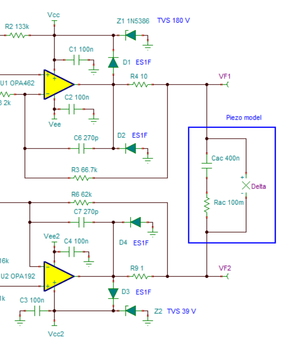
Figure 2-3 shows the output sections for two well-protected op amp piezo drivers. In each case, a TVS diode having a voltage just above the operating supply voltage is added at VCC1 and VCC2 pins. Zener diodes are shown in the schematic for illustrative purposes; a 180-V diode for the OPA462, and a 39-V diode for the OPA192. Fast recovery 1-A/300-V rectifier diodes are then connected from each op amp output pin to the supply pins. These diodes are normally off, but one or more may become forward biased and turn on during a voltage transient event. The ON rectifier diode will direct the current generated during the event to the corresponding TVS diode. The forward voltage of the rectifier diode will clamp the voltage across the output transistor of the op amp to a safe, low voltage, while the TVS clamps the supply voltage at its rated breakdown voltage.
 Figure 2-3 Fast Rectifier Diodes D1 – D4 and
TVS Diodes Z1 and Z2 Added to Protect U1 and U2 Outputs