SBOA527 November 2021 INA901-SP
3 High-Side Implementation
From the successful model on the low side, an inverted analog of the previous circuit may be realized to also implement such a design on the high side. However, a new challenge is observed for this design: for the previous low-side design, current flows from the supply pin towards the common-mode voltage, which is held to approximately 0 V. For a high-side implementation, the current must flow in the same direction across a resistor populated on the IN– leg, which in this circumstance is from the common-mode voltage to the ground. If the intended common mode is to be held constant, then the design is trivial, and a simple resistor to GND may designed as in the low-side case. However, for high-side designs, this is rarely the case, and large swings in the common-mode voltage result in proportionally large swings to the current that produces the desired offset. This makes the design goal clear: a constant current source is needed, utilizing parts that are readily available for space applications.
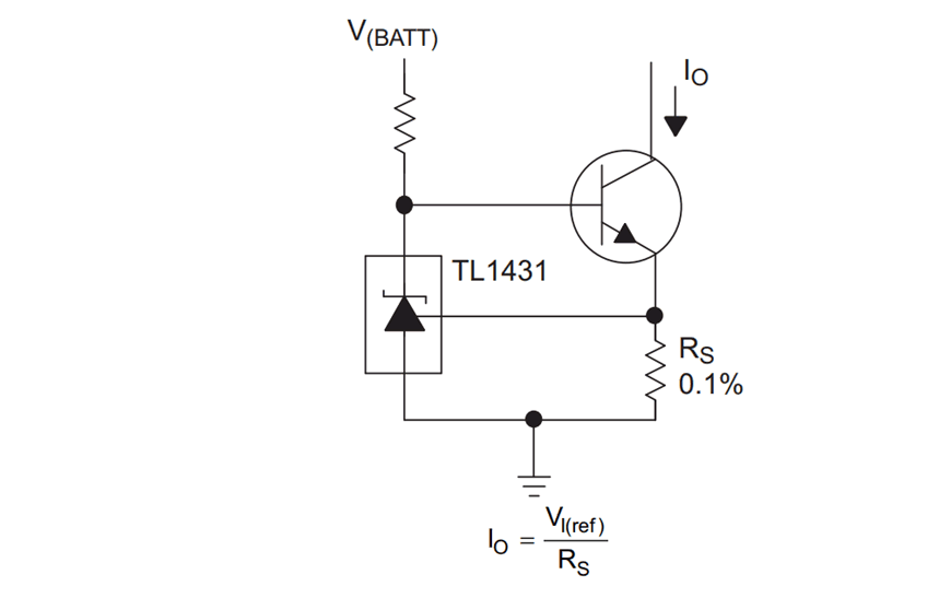
To design a current sink on the IN– sense line, there are several potential topologies, but this is easily achievable with a TL1431-SP programmable reference and a corresponding BJT NPN transistor.
 Figure 3-1 TL1431-SP Precision Constant Current Sink Schematic
As demonstrated in TL1431-SP Precision Constant Current Sink Schematic, this design uses a precision resistor to achieve the sink current needed. Conveniently, as the default reference of the TL1431-SP is 2.5 V, the offset current of the previous design can be recreated with a 1-kΩ resistor, for RS.
The tradeoff to this design is that, as stated, the reference voltage of the TL1431-SP is 2.5 V, which means that the power dissipated across the chosen NPN transistor is:
Note that the power dissipated in the BJT is directly proportional to the offset current, allowing an optimal point to be reached between power dissipated in the BJT and the offset created for the INA901. However, even in cases where the BJT power must be maximized, this power loss should be manageable. For the proposed design, even for valid common modes above the design case, the worst-case power dissipation is calculated to be:
The previous analysis also allows two additional observations. First, the NPN chosen for the application must be VCE voltage rated for at least the common-mode voltage less 2.5 V, although an additional margin for potential common-mode transients is advised to provide robust performance and minimize potential failures. Second, similar to the low-side design, this shows that this circuit also has a limitation based on directionality of current, and is only suited for applications of VCM > 2.5 V.
Similar to the low-side design, it is advised that the offset current be established such that the sense voltage of the INA901 is maintained above 20 mV to ensure optimal performance. From here, the analysis follows that of the low-side circuit, with the exception that the offset is created on the IN– leg of the amplifier.
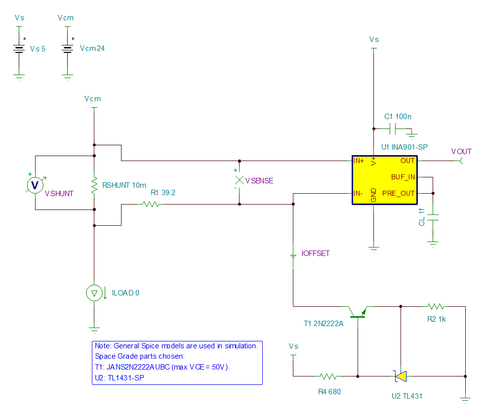
 Figure 3-2 INA901-SP High-Side Bidirectional Implementation
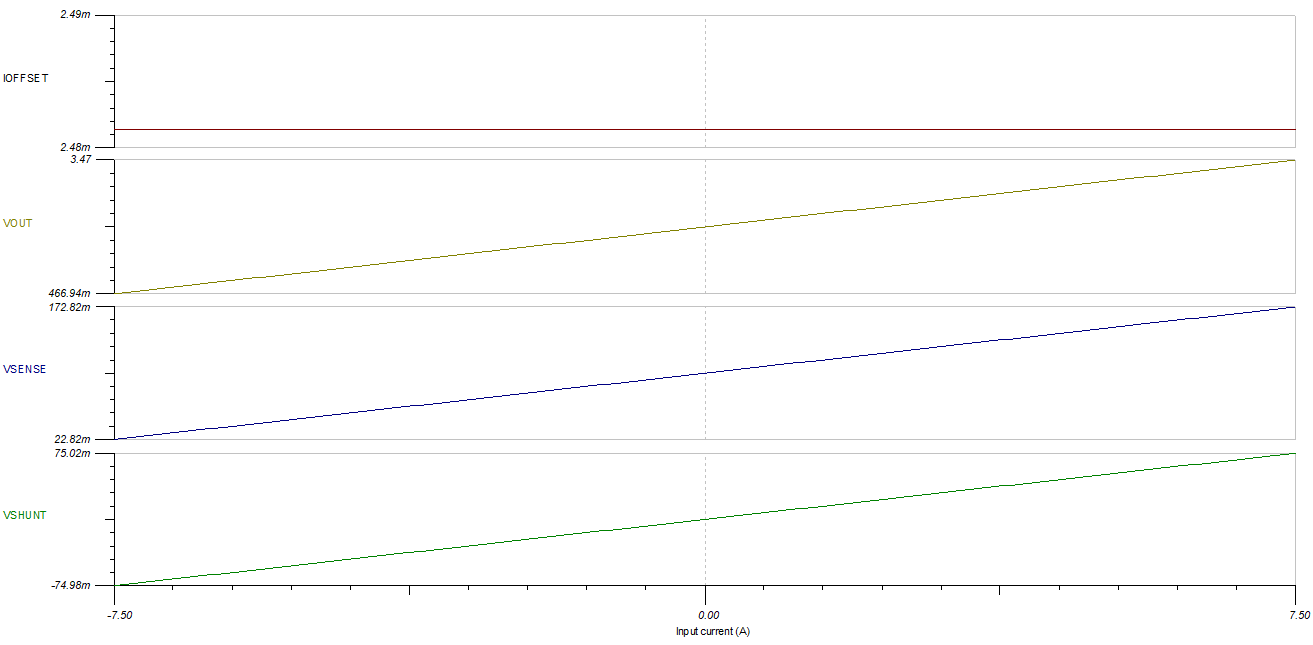
The previous resulting steps provide the needed results for a high-side approach. The designed 2.5 mA ideal IOFFSET and chosen 39.2-Ω resistor for R1 combine to produce an ideal 98-mV RTI input voltage, which shifts the VSENSE range again to 23 mV and 173 mV. INA901-SP High Side Simulation Results shows the TINA-TI simulated output results.
 Figure 3-3 INA901-SP High-Side Simulation Results
This design was also prototyped alongside the low-side design for real-world comparison. Table 3-1 through Table 3-3 display data captured via this topology at ambient temperature, as well as temperature extremes of –55°C and 125°C. For these data sets, E96 resistors of 0.1% tolerance were again utilized, maintaining a temperature coefficient of 50 ppm/°C. The BJT utilized here is 2N2222A, which has a maximum collector-emitter voltage of 40 V, which provides sufficient margin for the 24-VCM test condition. Space versions of this part exist (JANS2N2222AUBC) with even higher VCE capabilities (50 V), and was a motivation for this choice.
ILOAD (A) | VSHUNT, Meas. (V) | Output Voltage, Meas. Ideal (V) | VOUT, Meas. (V) | Error (%) | VOUT, | Error, |
|---|---|---|---|---|---|---|
–7.5 | –0.074994 | 0.46012 | 0.45511 | –1.09% | 0.46215 | 0.44% |
–6.25 | –0.062494 | 0.71012 | 0.70474 | –0.76% | 0.71178 | 0.23% |
–5 | –0.049994 | 0.96012 | 0.95445 | –0.59% | 0.96149 | 0.14% |
–3.75 | –0.037494 | 1.21012 | 1.2041 | –0.50% | 1.21114 | 0.08% |
–2.5 | –0.024994 | 1.46012 | 1.4538 | –0.43% | 1.46084 | 0.05% |
–1.25 | –0.012493 | 1.71014 | 1.7035 | –0.39% | 1.71054 | 0.02% |
0 | 0.000007 | 1.96014 | 1.9531 | –0.36% | 1.96014 | 0.00% |
1.25 | 0.012507 | 2.21014 | 2.2028 | –0.33% | 2.20984 | –0.01% |
2.5 | 0.025007 | 2.46014 | 2.4525 | –0.31% | 2.45954 | –0.02% |
3.75 | 0.037507 | 2.71014 | 2.7022 | –0.29% | 2.70924 | –0.03% |
5 | 0.050007 | 2.96014 | 2.9519 | –0.28% | 2.95894 | –0.04% |
6.25 | 0.062507 | 3.21014 | 3.2015 | –0.27% | 3.20854 | –0.05% |
7.5 | 0.075008 | 3.46016 | 3.4512 | –0.26% | 3.45824 | –0.06% |
ILOAD (A) | VSHUNT, Meas. (V) | Output Voltage, Meas. Ideal (V) | VOUT, Meas. (V) | Error (%) | VOUT, | Error, |
|---|---|---|---|---|---|---|
–7.5 | –0.074994 | 0.46012 | 0.45782 | –0.50% | 0.46486 | 1.03% |
–6.25 | –0.062494 | 0.71012 | 0.70733 | –0.39% | 0.71437 | 0.60% |
–5 | –0.049994 | 0.96012 | 0.95689 | –0.34% | 0.96393 | 0.40% |
–3.75 | –0.037494 | 1.21012 | 1.2065 | –0.30% | 1.21354 | 0.28% |
–2.5 | –0.024994 | 1.46012 | 1.4561 | –0.28% | 1.46314 | 0.21% |
–1.25 | –0.012494 | 1.71012 | 1.7057 | –0.26% | 1.71274 | 0.15% |
0 | 0.000006 | 1.96012 | 1.9553 | –0.25% | 1.96234 | 0.11% |
1.25 | 0.012504 | 2.21008 | 2.205 | –0.23% | 2.21204 | 0.09% |
2.5 | 0.025004 | 2.46008 | 2.4547 | –0.22% | 2.46174 | 0.07% |
3.75 | 0.037504 | 2.71008 | 2.7044 | –0.21% | 2.71144 | 0.05% |
5 | 0.050004 | 2.96008 | 2.9541 | –0.20% | 2.96114 | 0.04% |
6.25 | 0.062505 | 3.2101 | 3.2037 | –0.20% | 3.21074 | 0.02% |
7.5 | 0.075004 | 3.46008 | 3.4535 | –0.19% | 3.46054 | 0.01% |
ILOAD (A) | VSHUNT, Meas. (V) | Output Voltage, Meas. Ideal (V) | VOUT, Meas. (V) | Error (%) | VOUT, | Error, |
|---|---|---|---|---|---|---|
–7.5 | –0.074994 | 0.46012 | 0.4447 | –3.35% | 0.45174 | –1.82% |
–6.25 | –0.062494 | 0.71012 | 0.69431 | –2.23% | 0.70135 | –1.24% |
–5 | –0.049994 | 0.96012 | 0.94398 | –1.68% | 0.95102 | –0.95% |
–3.75 | –0.037493 | 1.21014 | 1.1937 | –1.36% | 1.20074 | –0.78% |
–2.5 | –0.024993 | 1.46014 | 1.4433 | –1.15% | 1.45034 | –0.67% |
–1.25 | –0.012494 | 1.71012 | 1.693 | –1.00% | 1.70004 | –0.59% |
0 | 0.000006 | 1.96012 | 1.9429 | –0.88% | 1.94994 | –0.52% |
1.25 | 0.012506 | 2.21012 | 2.1925 | –0.80% | 2.19954 | –0.48% |
2.5 | 0.025006 | 2.46012 | 2.4422 | –0.73% | 2.44924 | –0.44% |
3.75 | 0.037506 | 2.71012 | 2.6919 | –0.67% | 2.69894 | –0.41% |
5 | 0.050006 | 2.96012 | 2.9417 | –0.62% | 2.94874 | –0.38% |
6.25 | 0.062507 | 3.21014 | 3.1914 | –0.58% | 3.19844 | –0.36% |
7.5 | 0.075006 | 3.46012 | 3.4411 | –0.55% | 3.44814 | –0.35% |
This design also operates in a unidirectional manner, similar to the low-side approach; therefore, the offset should be calibrated for best results. Unlike the low-side approach, because the offset current is set via a constant current source, the offset voltage is maintained independently of the sense voltage, although there may still be some deviation due to temperature drift in R2. This can be optimized through low-drift, high-precision resistor selection.
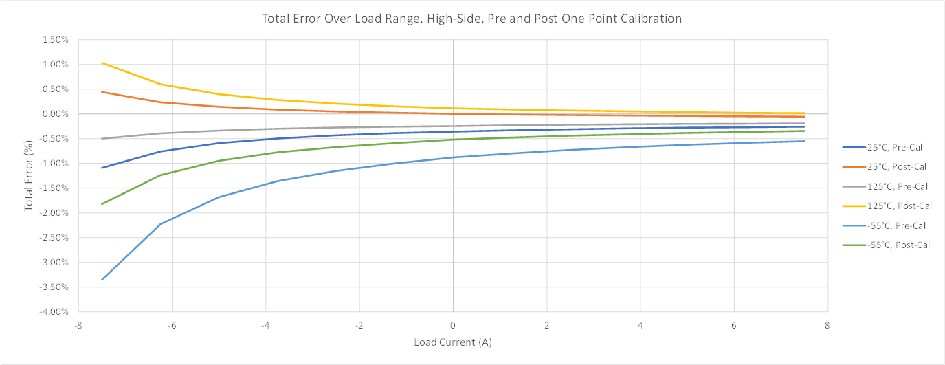
Table 3-1 through Table 3-3 list the actual data points captured from bench testing, and list the error compared against calculated design ideals, as well as adjusted error from a one-point calibration performed in post. It can be observed that by performing this calibration, error can be improved upon for the majority of the measurement range, and the linear error present in the low-side design due to the shifting sense node is eliminated.
 Figure 3-4 High-Side, Bidirectional Error Over Range, Pre- and Post-Calibration