SBOS957F February 2022 – October 2025 OPA2328 , OPA328 , OPA4328
PRODMIX
- 1
- 1 Features
- 2 Applications
- 3 Description
- 4 Pin Configuration and Functions
- 5 Specifications
- 6 Detailed Description
- 7 Application and Implementation
- 8 Device and Documentation Support
- 9 Revision History
- 10Mechanical, Packaging, and Orderable Information
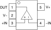
4 Pin Configuration and Functions
 Figure 4-1 OPA328 DBV Package
5-Pin SOT-23
(Top View)
 Figure 4-2 OPA328S DBV Package
(Preview)
Figure 4-2 OPA328S DBV Package
(Preview)6-Pin SOT-23
(Top View)
Pin Functions:
OPA328 and OPA328S
| PIN | TYPE | DESCRIPTION | ||
|---|---|---|---|---|
| NAME | OPA328 | OPA328S | ||
| –IN | 4 | 4 | Input | Negative (inverting) input |
| +IN | 3 | 3 | Input | Positive (noninverting) input |
| OUT, VOUT | 1 | 1 | Output | Output |
| SHDN | — | 5 | Input | Shutdown, active low |
| V– | 2 | 2 | Power | Negative (lowest) power supply |
| V+ | 5 | 6 | Power | Positive (highest) power supply |
 Figure 4-3 OPA2328 D and DGK
Package
Figure 4-3 OPA2328 D and DGK
Package8-pin SOIC and and VSSOP
(Top View)
 Figure 4-5 OPA2328 YBJ Package
24-Pin DSBGA
(Top View)
 Figure 4-4 OPA2328 DRG Package,
 8-Pin WSON
(Top View)
Pin Functions:
OPA2328
| PIN | TYPE | DESCRIPTION | ||
|---|---|---|---|---|
| NAME | D (SOIC), DGK (VSSOP), DRG (WSON) | YBJ (DSBGA) | ||
| –IN A | 2 | A1 | Input | Inverting input, channel A |
| +IN A | 3 | A3 | Input | Noninverting input, channel A |
| –IN B | 6 | E1 | Input | Inverting input, channel B |
| +IN B | 5 | E3 | Input | Noninverting input, channel B |
| OUT A | 1 | A2 | Output | Output, channel A |
| OUT B | 7 | E2 | Output | Output, channel B |
| SHDN | — | D5 | Input | Shutdown control for both channel A and channel B. Logic level low = amplifiers enabled. Logic level high = amplifiers disabled. |
| V– | 4 | C5, E5 | Power | Negative (lowest) power supply |
| V+ | 8 | A4, A5, B5, E4 | Power | Positive (highest) power supply |
| DNC | — | B1, B2, B3, B4, C1, C2, C4, D1, D2, D3, D4 | — | Do not connect |
 Figure 4-6 OPA4328 PW Package
14-Pin TSSOP
(Top View)
Table 4-1 Pin Functions: OPA4328
| PIN | TYPE | DESCRIPTION | |
|---|---|---|---|
| NAME | NO. | ||
| PW (TSSOP) | |||
| –IN A | 2 | Input | Inverting input, channel A |
| +IN A | 3 | Input | Noninverting input, channel A |
| –IN B | 6 | Input | Inverting input, channel B |
| +IN B | 5 | Input | Noninverting input, channel B |
| –IN C | 9 | Input | Inverting input, channel C |
| +IN C | 10 | Input | Noninverting input, channel C |
| –IN D | 13 | Input | Inverting input, channel D |
| +IN D | 12 | Input | Noninverting input, channel D |
| OUT A | 1 | Output | Output, channel A |
| OUT B | 7 | Output | Output, channel B |
| OUT C | 8 | Output | Output, channel C |
| OUT D | 14 | Output | Output, channel D |
| V– | 11 | Power | Negative (lowest) power supply |
| V+ | 4 | Power | Positive (highest) power supply |