SBOU268 November   2021 OPA593


  1.   Trademarks
  2. 1Overview
    1. 1.1 Getting Started
      1. 1.1.1 Related Documentation From Texas Instruments
    2. 1.2 High-Voltage Warning and Safe Use
    3. 1.3 Electrostatic Discharge Caution
  3. 2Operation
    1. 2.1 Jumper Blocks, Jacks, and Test Points
    2. 2.2 Inputs
    3. 2.3 Outputs
    4. 2.4 Enable or Disable
    5. 2.5 Status Flags
      1. 2.5.1 Circuit Protection
  4. 3Application Circuits
    1. 3.1 Setting Dual-Supply or Single-Supply Operation
      1. 3.1.1 Dual-Supply Operation Configuration
      2. 3.1.2 Single-Supply Operation Configuration
    2. 3.2 Common Op-Amp Configurations
      1. 3.2.1 Inverting Gain of –10 V/V
        1. 3.2.1.1 External Connections for –10 V/V Inverting Gain Configuration
        2. 3.2.1.2 Inverting Gain of –10 V/V Configuration Electrical Performance
      2. 3.2.2 Noninverting Gain of +2 V/V
        1. 3.2.2.1 External Connections to OPA593EVM for Noninverting Gain Configuration
        2. 3.2.2.2 Noninverting Gain Configuration Electrical Performance
      3. 3.2.3 Gain of +10 V/V Difference Amplifier
        1. 3.2.3.1 Jumper Shunt Locations for Difference-Amplifier Configuration
        2. 3.2.3.2 Gain of 10 V/V Difference Amplifier Configuration Electrical Performance
      4. 3.2.4 Improved Howland Current Pump
        1. 3.2.4.1 Jumper Shunt Locations for Improved Howland Current Pump Configuration
  5. 4Schematic, PCB Layout, and Bill of Materials
    1. 4.1 EVM Schematic
      1. 4.1.1 EVM Default Configuration
    2. 4.2 PCB Layout
    3. 4.3 Bill of Materials

PCB Layout

Figure 4-3 and Figure 4-4 show the OPA593EVM PCB top-side and bottom-side views of the PCB layout, respectively.
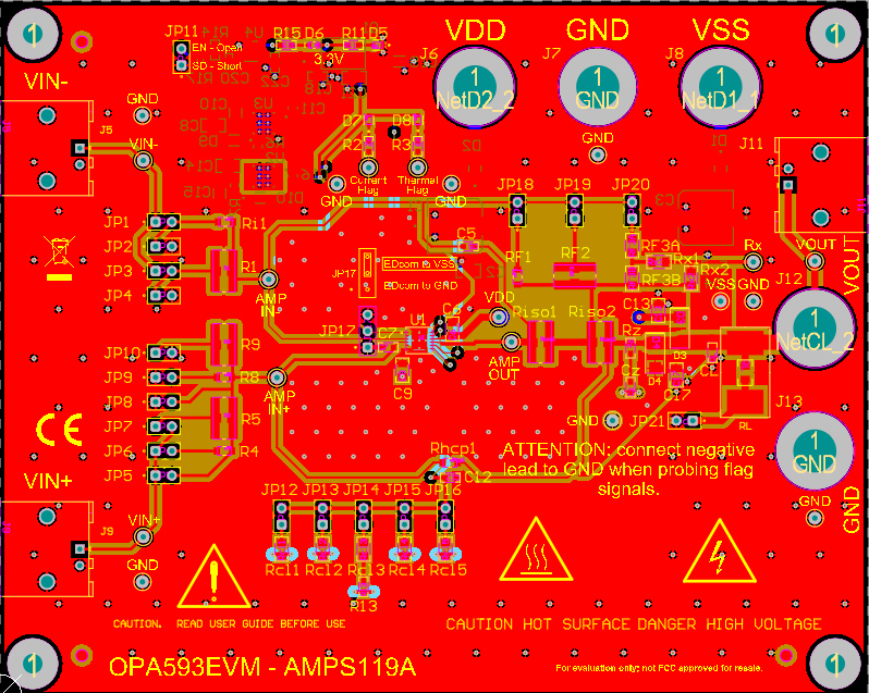
GUID-20211103-SS0I-75MZ-9WWX-TNKMRNZRBQL4-low.png Figure 4-3 Top-Side View of the OPA593EVM PCB
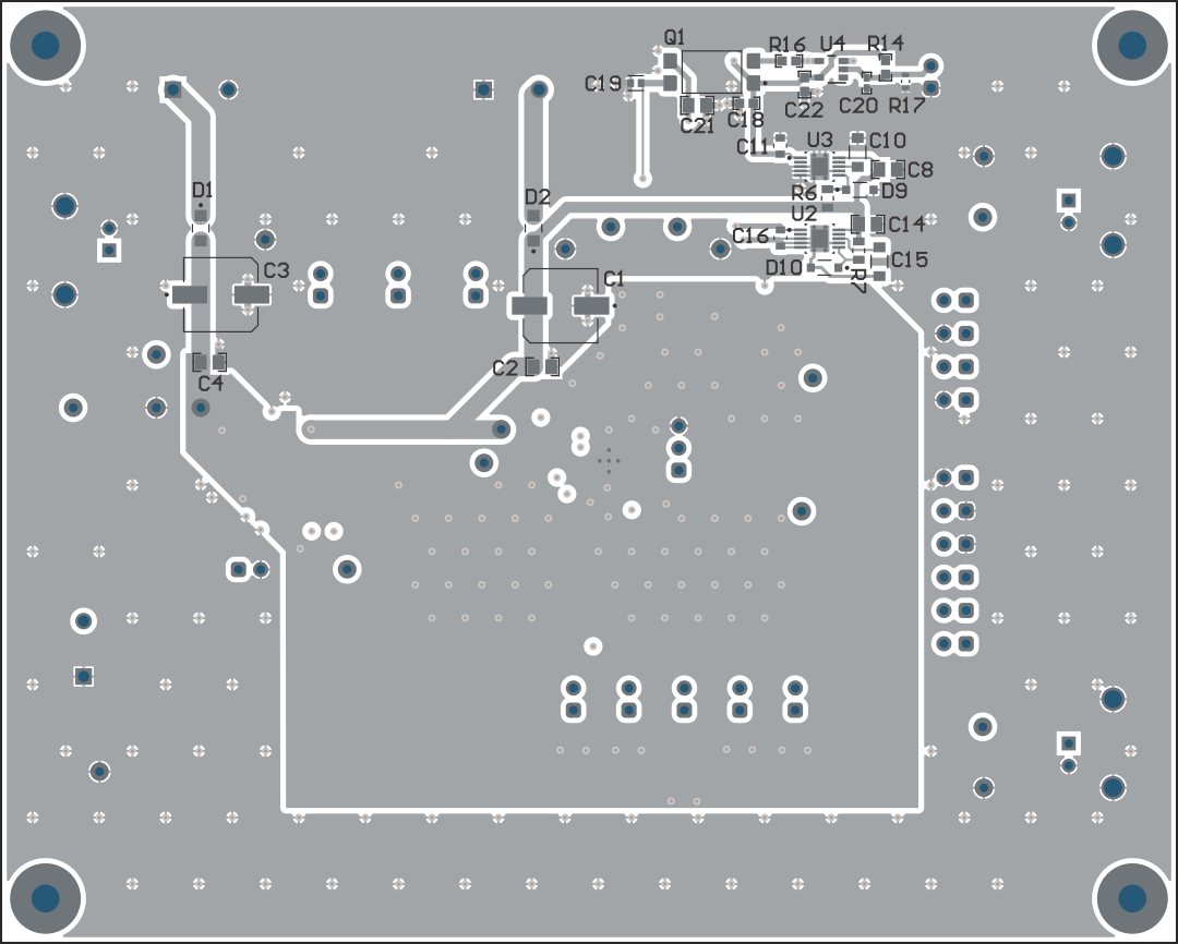
GUID-20211111-SS0I-B2SM-N41X-NSPFW5ZTG2MF-low.gif Figure 4-4 Bottom-Side View of the OPA593EVM PCB