SBVS233B January   2016  – June 2021 TPS7A84

PRODUCTION DATA  

  1. Features
  2. Applications
  3. Description
  4. Revision History
  5. Pin Configurations and Functions
  6. Specifications
    1. 6.1 Absolute Maximum Ratings
    2. 6.2 ESD Ratings
    3. 6.3 Recommended Operating Conditions
    4. 6.4 Thermal Information
    5. 6.5 Electrical Characteristics
    6. 6.6 Typical Characteristics
  7. Detailed Description
    1. 7.1 Overview
    2. 7.2 Functional Block Diagram
    3. 7.3 Feature Description
      1. 7.3.1  Low-Noise, High-PSRR Output
      2. 7.3.2  Integrated Resistance Network (ANY-OUT)
      3. 7.3.3  Bias Rail
      4. 7.3.4  Power-Good Function
      5. 7.3.5  Programmable Soft-Start
      6. 7.3.6  Internal Current Limit (ILIM)
      7. 7.3.7  Enable
      8. 7.3.8  Active Discharge Circuit
      9. 7.3.9  Undervoltage Lockout (UVLO)
      10. 7.3.10 Thermal Protection
    4. 7.4 Device Functional Modes
      1. 7.4.1 Operation with 1.1 V ≤ VIN < 1.4 V
      2. 7.4.2 Operation with 1.4 V ≤ VIN ≤ 6.5 V
      3. 7.4.3 Shutdown
  8. Application and Implementation
    1. 8.1 Application Information
      1. 8.1.1  Recommended Capacitor Types
      2. 8.1.2  Input and Output Capacitor Requirements (CIN and COUT)
      3. 8.1.3  Noise-Reduction and Soft-Start Capacitor (CNR/SS)
      4. 8.1.4  Feed-Forward Capacitor (CFF)
      5. 8.1.5  Soft-Start and In-Rush Current
      6. 8.1.6  Optimizing Noise and PSRR
      7. 8.1.7  Charge Pump Noise
      8. 8.1.8  ANY-OUT Programmable Output Voltage
      9. 8.1.9  ANY-OUT Operation
      10. 8.1.10 Increasing ANY-OUT Resolution for LILO Conditions
      11. 8.1.11 Current Sharing
      12. 8.1.12 Adjustable Operation
      13. 8.1.13 Sequencing Requirements
        1. 8.1.13.1 Sequencing with a Power-Good DC-DC Converter Pin
        2. 8.1.13.2 Sequencing with a Microcontroller (MCU)
      14. 8.1.14 Power-Good Operation
      15. 8.1.15 Undervoltage Lockout (UVLO) Operation
      16. 8.1.16 Dropout Voltage (VDO)
      17. 8.1.17 Behavior when Transitioning from Dropout into Regulation
      18. 8.1.18 Load Transient Response
      19. 8.1.19 Negatively-Biased Output
      20. 8.1.20 Reverse Current Protection
      21. 8.1.21 Power Dissipation (PD)
      22. 8.1.22 Estimating Junction Temperature
      23. 8.1.23 Recommended Area for Continuous Operation (RACO)
    2. 8.2 Typical Applications
      1. 8.2.1 Low-Input, Low-Output (LILO) Voltage Conditions
        1. 8.2.1.1 Design Requirements
        2. 8.2.1.2 Detailed Design Procedure
        3. 8.2.1.3 Application Curves
      2. 8.2.2 Typical Application for a 5.0-V Rail
        1. 8.2.2.1 Design Requirements
        2. 8.2.2.2 Detailed Design Procedure
        3. 8.2.2.3 Application Curves
  9. Power Supply Recommendations
  10. 10Layout
    1. 10.1 Layout Guidelines
      1. 10.1.1 Board Layout
    2. 10.2 Layout Example
  11. 11Device and Documentation Support
    1. 11.1 Device Support
      1. 11.1.1 Development Support
        1. 11.1.1.1 Evaluation Modules
        2. 11.1.1.2 Spice Models
      2. 11.1.2 Device Nomenclature
    2. 11.2 Documentation Support
      1. 11.2.1 Related Documentation
    3. 11.3 Receiving Notification of Documentation Updates
    4. 11.4 Support Resources
    5. 11.5 Trademarks
    6. 11.6 Electrostatic Discharge Caution
    7. 11.7 Glossary
  12. 12Mechanical, Packaging, and Orderable Information

Typical Characteristics

at TA = 25°C, VIN = 1.4 V or VIN = VOUT(NOM) + 0.4 V (whichever is greater), VBIAS = open, VOUT(NOM) = 0.8 V, VEN = 1.1 V, COUT = 47 μF, CNR/SS = 0 nF, CFF = 0 nF, and PG pin pulled up to VIN with 100 kΩ (unless otherwise noted)
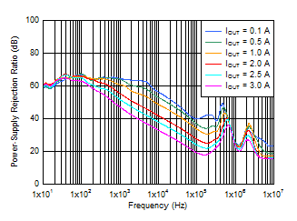
GUID-9D52F818-48F2-4D56-BDD4-BC3ABEC35CCF-low.gif
VIN = 1.1 V, VBIAS = 5 V, COUT = 47 μF || 10 μF || 10 μF,
CNR/SS = 10 nF, CFF = 10 nF
Figure 6-1 PSRR vs Frequency and IOUT
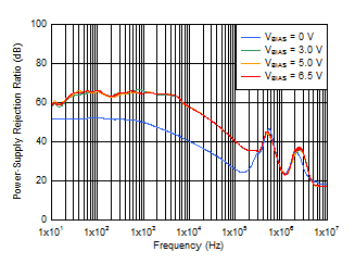
GUID-28C9CE41-97D5-4018-B9C2-7BC560FA2B19-low.gif
VIN = 1.4 V, IOUT = 1 A, COUT = 47 μF || 10 μF || 10 μF,
CNR/SS = 10 nF, CFF = 10 nF
Figure 6-3 PSRR vs Frequency and VBIAS
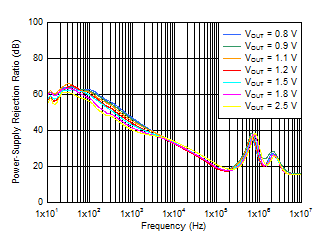
GUID-E68129AD-8936-4691-BE74-D579FA8AA367-low.gif
VIN = VOUT + 0.3 V, VBIAS = 5.0 V, IOUT = 3 A, COUT = 47 μF || 10 μF || 10 μF, CNR/SS = 10 nF, CFF = 10 nF
Figure 6-5 PSRR vs Frequency and VOUT With Bias
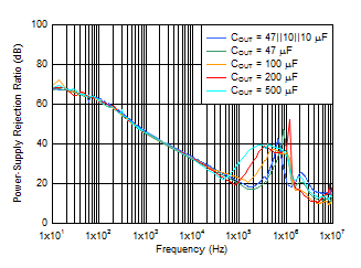
GUID-A2452D28-EC0C-4E98-B17B-AA47BD0A90A8-low.gif
VIN = VOUT + 0.3 V, VOUT = 1 V, IOUT = 3 A, CNR/SS = 10 nF, CFF = 10 nF
Figure 6-7 PSRR vs Frequency and COUT
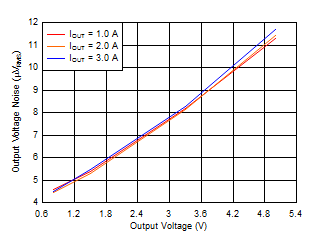
GUID-236AB31B-285F-4F91-84B7-9032165EA302-low.gif
VIN = VOUT + 0.3 V and VBIAS = 5 V for VOUT ≤ 2.2 V,
COUT = 47 μF || 10 μF || 10 μF, CNR/SS = 10 nF, CFF = 10 nF, RMS noise BW = 10 Hz to 100 kHz
Figure 6-9 Output Voltage Noise vs Output Voltage
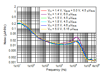
GUID-238436C2-4B8F-4DB9-A47C-E71746DAE844-low.gif
IOUT = 3 A, COUT = 47 μF || 10 μF || 10 μF, CNR/SS = 10 nF,
CFF = 10 nF, RMS noise BW = 10 Hz to 100 kHz
 
Figure 6-11 Output Noise vs Frequency and Input Voltage
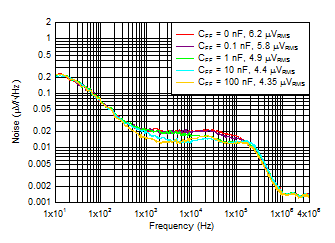
GUID-D9A93502-9472-49AD-BCDB-255B185B1570-low.gif
VIN = VOUT + 0.3 V, VBIAS = 5 V, IOUT = 3 A, sequencing with a dc/dc converter and PG, COUT = 47 μF || 10 μF || 10 μF, CNR/SS = 10 nF, RMS noise BW = 10 Hz to 100 kHz
Figure 6-13 Output Noise vs Frequency and CFF
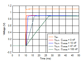
GUID-465D7404-60E6-46AA-8E8D-8F80A0F080A1-low.gif
VIN = 1.2 V, VOUT = 0.9 V, VBIAS = 5.0 V, IOUT = 3 A,
COUT = 47 μF || 10 μF || 10 μF, CFF = 10 nF
Figure 6-15 Start-Up Waveform vs Time and CNR/SS
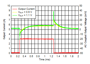
GUID-7F78F542-405F-4C9F-A48E-35C70EB613D4-low.gif
IOUT, DC = 100 mA, COUT = 47 μF || 10 μF || 10 μF,
CNR/SS = CFF = 10 nF, slew rate = 1 A/μs
Figure 6-17 Load Transient vs Time and VOUT Without Bias
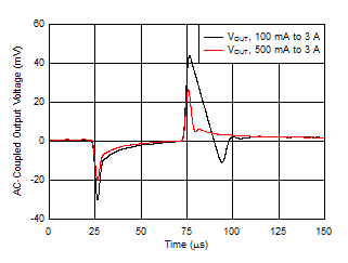
GUID-EB76E430-687F-4F22-82BE-6C9DAFF50CEB-low.gif
VIN = 1.2 V, VBIAS = 5.0 V, COUT = 47 μF || 10 μF || 10 μF, CNR/SS = CFF = 10 nF, slew rate = 1 A/μs
Figure 6-19 Load Transient vs Time and DC Load (VOUT = 0.9 V)
GUID-25177319-8B9F-4F9C-890F-DD9CAC28F867-low.gif
IOUT = 3 A, VBIAS = 6.5 V
Figure 6-21 Dropout Voltage vs Input Voltage With Bias
GUID-BD6289C7-E229-4161-9E19-1D7754BE4258-low.gif
VIN = 1.1 V, VBIAS = 3 V
Figure 6-23 Dropout Voltage vs Output Current With Bias
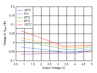
GUID-BA2D8F2B-CCFE-4209-A900-F3F97FEF7904-low.gif
IOUT = 100 mA to 3 A
Figure 6-25 Load Regulation vs Output Voltage
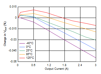
GUID-61DE5338-FE17-4FAA-ADED-6FDB912F823C-low.gif
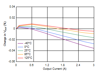
VIN = 3.8 V
Figure 6-27 Load Regulation (3.3-V Output)
GUID-E8C76F51-B4BE-4CC9-9CE0-005C5476C848-low.gif
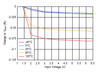
VOUT = 0.8 V, VBIAS = 0 V, IOUT = 5 mA
Figure 6-29 Line Regulation Without Bias
GUID-04E5FD24-D935-4B89-B8A1-564552ABB964-low.gif
IOUT = 5 mA
Figure 6-31 Line Regulation (5-V Output)
GUID-208903F6-8F41-4404-A4F0-5B0B95B3EAC8-low.gif
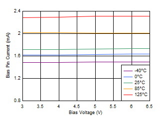
VIN = 1.1 V, IOUT = 5 mA
Figure 6-33 Quiescent Current vs Bias Voltage
GUID-617BF807-1D3A-49AF-92BF-AC04EAC02741-low.gif
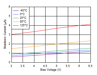
VIN = 1.1 V
Figure 6-35 Shutdown Current vs Bias Voltage
GUID-5151B53B-DF43-46A1-B635-8029A3F7F5C3-low.gif
 
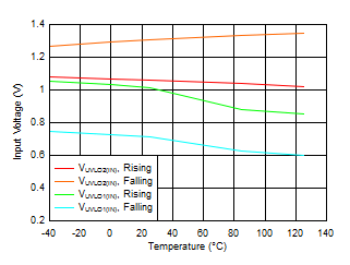
Figure 6-37 VIN UVLO vs Temperature
GUID-D018BA10-B298-4969-BFD6-0675FFC96CEA-low.gif
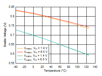
VIN = 1.4 V, 6.5 V
Figure 6-39 Enable Threshold vs Temperature
GUID-647FE270-A912-4DC6-B1A6-68C8D7E675B8-low.gif
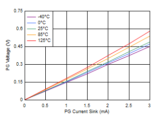
VIN = 6.5 V
Figure 6-41 PG Voltage vs PG Current Sink
GUID-AE743FB6-0A54-4F7C-8290-1489E2E0FD79-low.gif
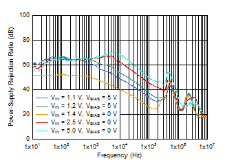
IOUT = 3 A, VBIAS = 5 V, COUT = 47 μF || 10 μF || 10 μF,
CNR/SS = 10 nF, CFF = 10 nF
Figure 6-2 PSRR vs Frequency and VIN With Bias
GUID-C8080EF1-A407-467B-957D-5B6D9FB409DA-low.gif
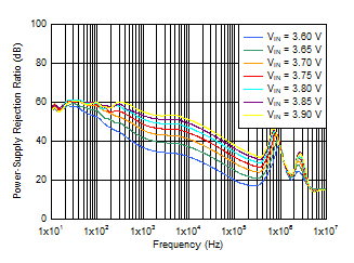
IOUT = 1 A, COUT = 47 μF || 10 μF || 10 μF, CNR/SS = 10 nF,
CFF = 10 nF
Figure 6-4 PSRR vs Frequency and VIN
GUID-8E8126B6-2B41-4AC2-9D51-03F3055848D4-low.gif
IOUT = 3 A, COUT = 47 μF || 10 μF || 10 μF, CNR/SS = 10 nF,
CFF = 10 nF
Figure 6-6 PSRR vs Frequency and VIN for VOUT = 3.3 V
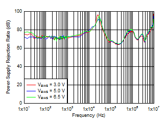
GUID-8F8EA0D8-BC98-48B5-9E2C-84ECB76D647B-low.gif
VIN = VOUT + 0.3 V, VOUT = 1 V, IOUT = 3 A,
COUT = 47 μF || 10 μF || 10 μF, CNR/SS = 10 nF, CFF = 10 nF
Figure 6-8 VBIAS PSRR vs Frequency
GUID-58D0942D-A438-4C7C-804B-853A983FBADB-low.gif
VIN = VOUT + 0.3 V and VBIAS = 5 V for VOUT ≤ 2.2 V,
IOUT = 3 A, COUT = 47 μF || 10 μF || 10 μF, CNR/SS = 10 nF, CFF = 10 nF, RMS noise BW = 10 Hz to 100 kHz
Figure 6-10 Output Noise vs Frequency and Output Voltage
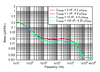
GUID-238DCCAB-762A-4DE5-9ADC-025AF89A3C8B-low.gif
VIN = VOUT + 0.3 V, VBIAS = 5 V, IOUT = 3 A, COUT = 47 μF ||
10 μF || 10 μF, CFF = 10 nF, RMS noise BW = 10 Hz to
100 kHz
Figure 6-12 Output Noise vs Frequency and CNR/SS
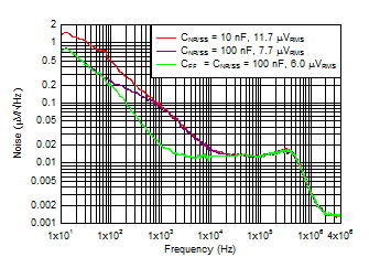
GUID-247904BC-5FD3-429B-A1AB-8038982C6183-low.gif
IOUT = 3 A, COUT = 47 μF || 10 μF || 10 μF, CFF = 10 nF,
RMS noise BW = 10 Hz to 100 kHz
 
Figure 6-14 Output Noise at 5.0-V Output
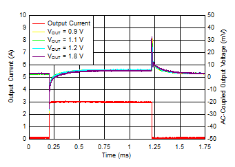
GUID-49B854A4-81F5-4662-B3B7-684241D3C067-low.gif
VIN = VOUT + 0.3 V, VBIAS = 5 V, IOUT, DC = 100 mA, slew rate = 1 A/μs, CNR/SS = CFF = 10 nF, COUT = 47 μF || 10 μF || 10 μF
Figure 6-16 Load Transient vs Time and VOUT With Bias
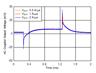
GUID-AEFDB9DF-2347-4917-810C-B4789198AB4F-low.gif
VOUT = 5 V, IOUT, DC = 100 mA, IOUT = 100 mA to 3 A,
COUT = 47 μF || 10 μF || 10 μF, CNR/SS = CFF = 10 nF
Figure 6-18 Load Transient vs Time and Slew Rate
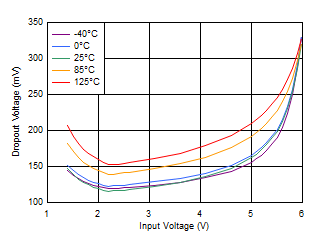
GUID-C3D48291-FB12-4F4A-9609-C599BADBCF5C-low.gif
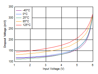
IOUT = 3 A, VBIAS = 0 V
 
Figure 6-20 Dropout Voltage vs Input Voltage Without Bias
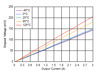
GUID-26F166B5-649A-43F7-BE43-ECE1F979E6B6-low.gif
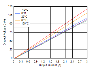
VIN = 1.4 V, VBIAS = 0 V
Figure 6-22 Dropout Voltage vs Output Current Without Bias
GUID-C5AD474A-D9E6-4312-B5FB-744EEDF54313-low.gif
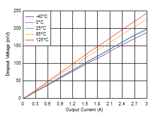
VIN = 5.5 V
Figure 6-24 Dropout Voltage vs Output Current (High VIN)
GUID-FF908E85-2CCC-4223-A586-5E39D0D47175-low.gif
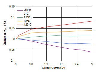
VIN = 1.4 V, VBIAS = 0 V
Figure 6-26 Load Regulation With Bias
GUID-73723F51-1FD4-4CBF-BA0E-68D6A65ED1EC-low.gif
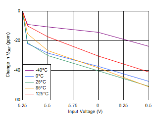
VIN = 5.5 V
Figure 6-28 Load Regulation (5-V Output)
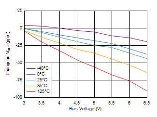
GUID-D4509822-0DC2-445F-BD3D-655517FFCAA9-low.gif
VOUT = 0.8 V, VIN = 1.1 V, IOUT = 5 mA
Figure 6-30 Line Regulation Without Bias
GUID-D90F40C0-72AC-41FD-B5A6-A90D209A7AAC-low.gif
VBIAS = 0 V, IOUT = 5 mA
Figure 6-32 Quiescent Current vs Input Voltage
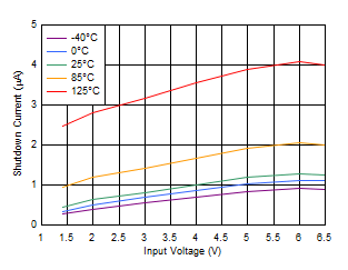
GUID-CE6AF4C1-E449-49BA-9574-0FD18487472D-low.gif
VBIAS = 0 V
Figure 6-34 Shutdown Current vs Input Voltage
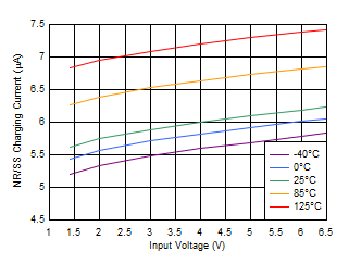
GUID-B83ED9B7-DB0C-4890-90B4-D8F31F9F38FB-low.gif
VBIAS = 0 V
Figure 6-36 INR/SS Current vs Input Voltage
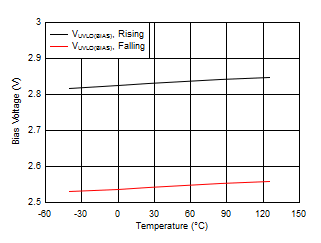
GUID-92461A0E-9034-47CE-A53F-2A85207A6C9D-low.gif
VIN = 1.1 V
Figure 6-38 VBIAS UVLO vs Temperature
GUID-34A93A7E-AD55-41BB-8AC9-643B86B41E8A-low.gif
 
Figure 6-40 PG Voltage vs PG Current Sink
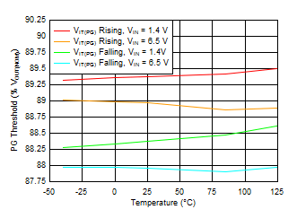
GUID-F61C53AC-134A-4DB2-A82B-B165D09F3512-low.gif
 
Figure 6-42 PG Threshold vs Temperature