SBVS475A March   2026  – June 2026 TPS7A43-Q1

PRODUCTION DATA  

  1.   1
  2. Features
  3. Applications
  4. Description
  5. Pin Configuration and Functions
  6. Specifications
    1. 5.1 Absolute Maximum Ratings
    2. 5.2 ESD Ratings
    3. 5.3 Recommended Operating Conditions
    4. 5.4 Thermal Information
    5. 5.5 Electrical Characteristics
    6. 5.6 Typical Characteristics
  7. Detailed Description
    1. 6.1 Overview
    2. 6.2 Functional Block Diagrams
    3. 6.3 Feature Description
      1. 6.3.1 MID_OUT Voltage Selection
      2. 6.3.2 Precision Enable
      3. 6.3.3 Dropout Voltage
      4. 6.3.4 Current Limit
      5. 6.3.5 Thermal Shutdown
      6. 6.3.6 Power Good
    4. 6.4 Device Functional Modes
      1. 6.4.1 Device Functional Mode Comparison
      2. 6.4.2 Normal Operation
      3. 6.4.3 Dropout Operation
      4. 6.4.4 Disabled
  8. Application and Implementation
    1. 7.1 Application Information
      1. 7.1.1 MID_OUT Voltage Setting
      2. 7.1.2 OUT-Only Operation (Use Without MID_OUT)
      3. 7.1.3 MID_OUT-Only Operation (Use Without OUT)
      4. 7.1.4 Adjustable Device Feedback Resistors
      5. 7.1.5 Recommended Capacitor Types
      6. 7.1.6 Input and Output Capacitor Requirements
      7. 7.1.7 Power Dissipation (PD)
      8. 7.1.8 Estimating Junction Temperature
      9. 7.1.9 Operation Beyond Rated Output Current
    2. 7.2 Typical Application
      1. 7.2.1 Design Requirements
      2. 7.2.2 Detailed Design Procedure
      3. 7.2.3 Application Curves
    3. 7.3 Power Supply Recommendations
    4. 7.4 Layout
      1. 7.4.1 Layout Guidelines
      2. 7.4.2 Layout Examples
  9. Device and Documentation Support
    1. 8.1 Device Support
      1. 8.1.1 Development Support
        1. 8.1.1.1 Evaluation Modules
        2. 8.1.1.2 Spice Models
      2. 8.1.2 Device Nomenclature
    2. 8.2 Documentation Support
      1. 8.2.1 Related Documentation
    3. 8.3 Receiving Notification of Documentation Updates
    4. 8.4 Support Resources
    5. 8.5 Trademarks
    6. 8.6 Electrostatic Discharge Caution
    7. 8.7 Glossary
  10. Revision History
  11. 10Mechanical, Packaging, and Orderable Information

Typical Characteristics

at operating temperature TJ = 25°C, IOUT = 1mA, IMID_OUT = 0mA, VEN = 2V, VMVSEL1 = 0.9V, VMVSEL2 = 0.9V, CIN = 1μF, CMID_OUT = 4.7μF, COUT = 1μF, and VIN = VMID_OUT + 1.5V (unless otherwise noted)

TPS7A43-Q1 VOUT Accuracy vs IOUT
VOUT = 1.24V (adjustable)
Figure 5-1 VOUT Accuracy vs IOUT
TPS7A43-Q1 VMID_OUT Accuracy vs VIN
VMID_OUT = 12V
 
Figure 5-3 VMID_OUT Accuracy vs VIN
TPS7A43-Q1 VMID_OUT vs IMID_OUT
VMID_OUT = 12V
Figure 5-5 VMID_OUT vs IMID_OUT
TPS7A43-Q1 IGND vs
                            IOUT
VIN = 16.5V, VMID_OUT = 15V, VMVSEL1 = VMVSEL2 = 0V,
VOUT = 1.24V (adjustable)
Figure 5-7 IGND vs IOUT
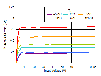
TPS7A43-Q1 ISHUTDOWN vs VIN
VEN = 1V
Figure 5-9 ISHUTDOWN vs VIN
TPS7A43-Q1 VDO(MID_OUT) vs IMID_OUT
VMID_OUT = 15V, VMVSEL1 = VMVSEL2 = 0V, IOUT = 0mA
 
Figure 5-11 VDO(MID_OUT) vs IMID_OUT
TPS7A43-Q1 Slow Start-Up
CIN = 0μF, VIN ramp rate = 45V/ms, VOUT = 3.3V,
IOUT = 10mA
Figure 5-13 Slow Start-Up
TPS7A43-Q1 Line Transient
VIN = 15V to 85V, VIN ramp rate = 10V/μs, VOUT = 3.3V,
IOUT = 10mA
Figure 5-15 Line Transient
TPS7A43-Q1 Line Transient
VIN = 15V to 85V, VIN ramp rate = 10V/μs, VOUT = 3.3V,
IOUT = 50mA
Figure 5-17 Line Transient
TPS7A43-Q1 Line Transient (VMID_OUT in Dropout)
VIN = 4V to 85V, VIN ramp rate = 1V/μs, VOUT = 3.3V,
IOUT = 50mA
Figure 5-19 Line Transient (VMID_OUT in Dropout)
TPS7A43-Q1 Line Transient (VMID_OUT in Dropout)
VIN = 4V to 85V, VIN ramp rate = 5V/μs, VOUT = 3.3V,
IOUT = 50mA
Figure 5-21 Line Transient (VMID_OUT in Dropout)
TPS7A43-Q1 Load Transient (Rising Edge)
VIN = 65V, VOUT = 3.3V, IOUT = 0mA to 50mA to 0mA,
IOUT slew rate = 1A/μs
Figure 5-23 Load Transient (Rising Edge)
TPS7A43-Q1 Load Transient (Rising Edge)
VIN = 65V, VOUT = 3.3V, IOUT = 1mA to 50mA to 1mA,
IOUT slew rate = 1A/μs
Figure 5-25 Load Transient (Rising Edge)
TPS7A43-Q1 Load Transient (MID_OUT)
VIN = 65V, VOUT = 3.3V, IMID_OUT = 0mA to 50mA to 0mA, IMID_OUT slew rate = 1A/μs, IOUT = 0mA
Figure 5-27 Load Transient (MID_OUT)
TPS7A43-Q1 Load Transient (MID_OUT)
VIN = 65V, VOUT = 3.3V, IMID_OUT = 1mA to 50mA to 1mA, IMID_OUT slew rate = 1A/μs, IOUT = 0mA
Figure 5-29 Load Transient (MID_OUT)
TPS7A43-Q1 Spectral Noise Density vs Frequency and COUT
VIN = 13V, VOUT = 3.3V, IOUT = 20mA,
VRMS bandwidth = 10Hz to 100kHz
Figure 5-31 Spectral Noise Density vs Frequency and COUT
TPS7A43-Q1 OUT PSRR vs Frequency and VIN
CIN = 0μF, VOUT = 3.3V, IOUT = 20mA
Figure 5-33 OUT PSRR vs Frequency and VIN
TPS7A43-Q1 MID_OUT PSRR vs Frequency and IMID_OUT
VIN = 13V, CIN = 0μF, VOUT = 3.3V, IOUT = 0mA
Figure 5-35 MID_OUT PSRR vs Frequency and IMID_OUT
TPS7A43-Q1 MID_OUT PSRR vs Frequency and CMID_OUT
VIN = 13V, CIN = 0μF, VOUT = 3.3V, IMID_OUT = 20mA,
IOUT = 0mA
Figure 5-37 MID_OUT PSRR vs Frequency and CMID_OUT
TPS7A43-Q1 VOUT Accuracy vs VIN
VOUT = 1.24V (adjustable)
Figure 5-2 VOUT Accuracy vs VIN
TPS7A43-Q1 VOUT vs IOUT
VOUT = 1.24V (adjustable)
Figure 5-4 VOUT vs IOUT
TPS7A43-Q1 IGND vs IOUT (MID_OUT in Dropout)
VIN = 11V, VOUT = 1.24V (adjustable)
 
Figure 5-6 IGND vs IOUT (MID_OUT in Dropout)
TPS7A43-Q1 IGND vs VIN
IOUT = 0mA
 
Figure 5-8 IGND vs VIN
TPS7A43-Q1 VDO(OUT) vs IOUT
VOUT = 1.24V (adjustable)
Figure 5-10 VDO(OUT) vs IOUT
TPS7A43-Q1 Fast
                        Start-Up
CIN = 0μF, VIN ramp rate = 10V/μs, VOUT = 3.3V,
IOUT = 10mA
Figure 5-12 Fast Start-Up
TPS7A43-Q1 Line Transient
VIN = 15V to 85V, VIN ramp rate = 10V/μs, VOUT = 3.3V,
IOUT = 50mA
Figure 5-14 Line Transient
TPS7A43-Q1 Line Transient
VIN = 15V to 85V, VIN ramp rate = 10V/μs, VOUT = 3.3V,
IOUT = 50mA
Figure 5-16 Line Transient
TPS7A43-Q1 Line Transient (VMID_OUT in Dropout)
VIN = 4V to 85V, VIN ramp rate = 1V/μs, VOUT = 3.3V,
IOUT = 50mA
Figure 5-18 Line Transient (VMID_OUT in Dropout)
TPS7A43-Q1 Line Transient (VMID_OUT in Dropout)
VIN = 4V to 85V, VIN ramp rate = 5V/μs, VOUT = 3.3V,
IOUT = 50mA
Figure 5-20 Line Transient (VMID_OUT in Dropout)
TPS7A43-Q1 Load Transient
VIN = 65V, VOUT = 3.3V, IOUT = 0mA to 50mA to 0mA,
IOUT slew rate = 1A/μs
Figure 5-22 Load Transient
TPS7A43-Q1 Load Transient
VIN = 65V, VOUT = 3.3V, IOUT = 1mA to 50mA to 1mA,
IOUT slew rate = 1A/μs
Figure 5-24 Load Transient
TPS7A43-Q1 Load Transient (MID_OUT)
VIN = 65V, VMID_OUT = 12V, IMID_OUT = 0mA to 50mA to 0mA, IMID_OUT slew rate = 1A/μs, IOUT = 0mA
Figure 5-26 Load Transient (MID_OUT)
TPS7A43-Q1 Load Transient (MID_OUT)
VIN = 65V, VMID_OUT = 12V, IMID_OUT = 1mA to 50mA to 1mA, IMID_OUT slew rate = 1A/μs, IOUT = 0mA
Figure 5-28 Load Transient (MID_OUT)
TPS7A43-Q1 Spectral Noise Density vs Frequency and IOUT
VIN = 13V, VOUT = 3.3V, VRMS bandwidth = 10Hz to 100kHz
 
Figure 5-30 Spectral Noise Density vs Frequency and IOUT
TPS7A43-Q1 OUT PSRR vs Frequency and IOUT
VIN = 13V, CIN = 0μF, VOUT = 3.3V
Figure 5-32 OUT PSRR vs Frequency and IOUT
TPS7A43-Q1 OUT PSRR vs Frequency and COUT
VIN = 13V, CIN = 0μF, VOUT = 3.3V, IOUT = 20mA
Figure 5-34 OUT PSRR vs Frequency and COUT
TPS7A43-Q1 MID_OUT PSRR vs Frequency and VIN
CIN = 0μF, VOUT = 3.3V, IMID_OUT = 20mA, IOUT = 0mA
 
Figure 5-36 MID_OUT PSRR vs Frequency and VIN
Note: The Typical Characteristics graphs show some data beyond rated output current. This data is not intended to serve as a recommendation to use the TPS7A43-Q1 beyond rated specifications. If using the device outside of the Recommended Operating Conditions, performance is not confirmed. See Operation Beyond Rated Output Current for more details.