SBVU074 November 2021
3.4 Optional Load Transient Circuit Operation
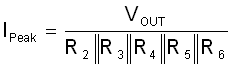
The TPS7A13EVM-057 evaluation module contains an optional high-performance load transient circuit to allow efficient testing of the TPS7A13 LDO load transient performance. To use the optional load transient circuit, install the correct components in accordance with the application. Modify the input and output capacitance connected to the TPS7A13 LDO to match the expected operating conditions. Determine the desired peak current to test, and modify the parallel resistor combination of R2, R3, R4, R5, and R6 as shown:
The slew rate of the load step can be adjusted by C11, R7, R8, and R9. In this section, only R8 and R9 are adjusted to set the slew rate. For a 0-mA to 300-mA load step, use Table 3-1 to select a value of R8 and R9 that results in the desired rise or fall time.
| R8 | R9 | Rise/Fall Time |
|---|---|---|
| 107 kΩ | 86.6 kΩ | 9.6 µs |
| 59 kΩ | 43.2 kΩ | 4.8 µs |
| 36.5 kΩ | 21.5 kΩ | 2.4 µs |
| 19.1 kΩ | 10.7 kΩ | 1.2 µs |
| 9.31 kΩ | 5.23 kΩ | 600 ns |
| 4.53 kΩ | 2.55 kΩ | 300 ns |
| 2.15 kΩ | 1.24 kΩ | 150 ns |
| 402 Ω | 267 Ω | 30 ns |
After the EVM is modified (if needed), connect a power supply to banana connectors J17 (VDD) and J21 (GND) with a 5-V DC supply and a 1-A DC current limit. As illustrated in Figure 3-3 and Figure 3-4, the TPS7A13 transient response is very fast and the output voltage recovers in well under 1 ms after the initial load transient. Therefore, use a load transient pulse duration limit of 1 ms to prevent excessive heating of the pulsed resistors (R2, R3, R4, R5, and R6). Configure a function generator for the 50-Ω output, in a 0-V DC to 5-V DC square pulse. If necessary, burst mode can be configured in the function generator for repetitive, low duty cycle, load transient testing.
A 2.49-kΩ resistor is installed on the EVM at R8, and a 2-kΩ resistor is installed on the EVM at R9. These resistors provide approximately 1 A/μs slew rate from 0 mA to 300 mA. Figure 3-3 and Figure 3-4 provide example test data with R8 = 2.49 kΩ and R9 = 2 kΩ. The red trace is the output voltage and the blue trace is the output current. J10 provides 1 mA of DC load current and R2, R3, R4, R5, and R6 provide 299 mA of pulsed load. The resulting test data shows a 1-mA to 300-mA load step on VOUT of the LDO, with only a 1-μF capacitor on the output of the LDO.
 Figure 3-3 TPS7A13EVM-057 Load
Transient Results: 1-mA to 300-mA Load Step
Figure 3-3 TPS7A13EVM-057 Load
Transient Results: 1-mA to 300-mA Load Step Figure 3-4 TPS7A13EVM-057 Load Transient Results: 300-mA to 1-mA Load Step