SCLA018A March   2019  – April 2021 SN74AVC4T774 , TXB0104


  1.   Trademarks
  2. 1Block Diagram
  3. 2Optimize System Controller to Wireless Module Interface
  4. 3Logic and Translation Use Cases
    1. 3.1 Logic Use Cases
      1. 3.1.1 Increase Number of Controller Outputs
      2. 3.1.2 Drive Indicator LEDs
      3. 3.1.3 Open-Drain Buffer
      4. 3.1.4 Debounce Switches and Buttons
      5. 3.1.5 Generate a Clock Signal from a Crystal Oscillator
    2. 3.2 Voltage Translation Use Cases
      1. 3.2.1 SPI Communication
      2. 3.2.2 GPIO Communication
      3. 3.2.3 I2C Communication
      4. 3.2.4 SD Card Communication
  5. 4Recommended Logic and Translation Families for Video Doorbells
    1. 4.1 AUP: Advanced Ultra-Low-Power CMOS Logic and Translation
    2. 4.2 AXC: Advanced Extremely Low-Voltage CMOS Translation
    3. 4.3 LVC: Low-Voltage CMOS Logic and Translation
  6. 5Revision History

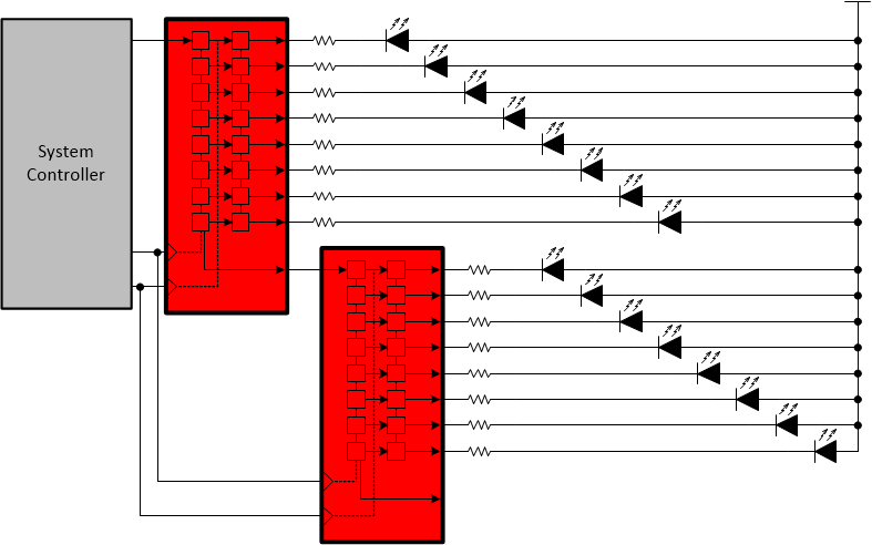
Increase Number of Controller Outputs

GUID-5F5A5308-9E21-42F6-A24E-D5BC27DE50BE-low.gifFigure 3-1 Using Two Shift Registers to Control 16 LEDs with Three Signals (Data, Shift Clock, and Output Register Clock)
  • As few as two outputs can be turned into 8 outputs with one serial-in parallel-out shift register.
  • Shift registers can be daisy chained for producing large numbers of outputs.
  • Low current (< 8 mA) LEDs can be driven directly.