SCPS260C August 2017 – February 2022 TIC12400-Q1
PRODUCTION DATA
- 1 Features
- 2 Applications
- 3 Description
- 4 Revision History
- 5 Pin Configuration and Functions
- 6 Specifications
- 7 Parameter Measurement Information
-
8 Detailed Description
- 8.1 Overview
- 8.2 Functional Block Diagram
- 8.3
Feature Description
- 8.3.1 VS Pin
- 8.3.2 VDD Pin
- 8.3.3 Device Initialization
- 8.3.4 Device Trigger
- 8.3.5 Device Reset
- 8.3.6 VS Under-Voltage (UV) Condition
- 8.3.7 VS Over-Voltage (OV) Condition
- 8.3.8 Switch Inputs Settings
- 8.3.9 Interrupt Generation and INT Assertion
- 8.3.10 Temperature Monitor
- 8.3.11 Parity Check and Parity Generation
- 8.3.12 Cyclic Redundancy Check (CRC)
- 8.4 Device Functional Modes
- 8.5 Programming
- 8.6 Register Maps
- 8.7 Programming Guidelines
- 9 Application Information Disclaimer
- 10Power Supply Recommendations
- 11Layout
- 12Device and Documentation Support
- 13Mechanical, Packaging, and Orderable Information
8.4.3.1 Clean Current Polling (CCP)
To detect resistor coded switches or reduce overall power consumption of the chip, a lower wetting current setting is recommended. However, certain system design requires 10 mA or higher cleaning current to clear oxide build-up on the mechanical switch contact surface when the current is applied to closed switches. A special type of polling, called the Clean Current Polling (CCP), can be used for this application.
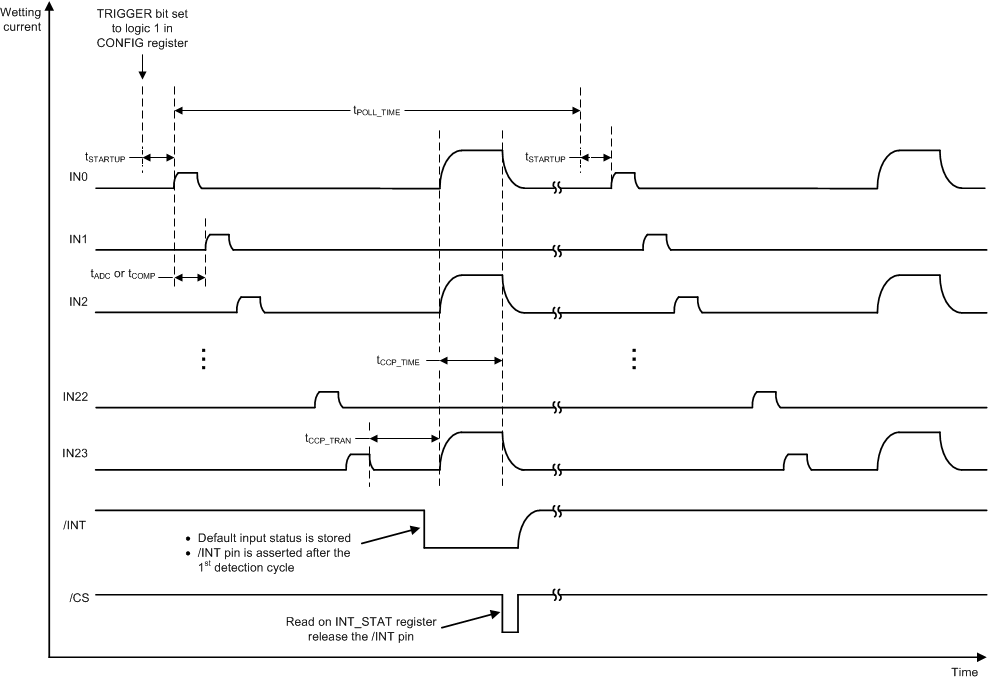
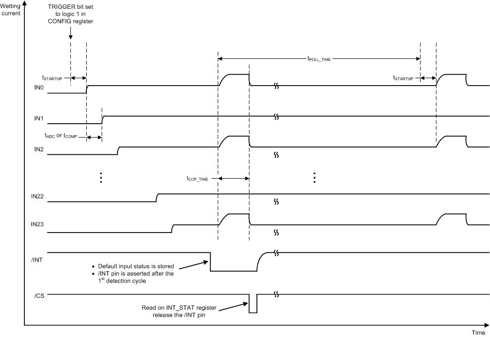
If CCP is enabled each polling cycle consists of two wetting current activation steps. The first step uses the wetting current setting configured in the WC_CFG0 and WC_CFG1 registers as in the continuous mode or polling mode. The second step (cleaning cycle) is activated simultaneously for all CCP enabled inputs at a time tCCP_TRAN after the normal polling step of the last enabled input. Interrupt generation and INT pin assertion is not impacted by the clean current pulses.
The wetting current and its active time for the cleaning cycle can be configured in the CCP_CFG0 register. The cleaning cycle can be disabled, if desired, for each individual input by programming the CCP_CFG1 register. CCP is available for both continuous mode and polling mode. To use the CCP feature, at least one input (standard or matrix) or the Section 8.4.3.3 has to be enabled.
Note: that although CCP can be enabled in Matrix polling mode, it is not an effective way to clean the matrix switch contact, since the current supplied from the TIC12400-Q1 is divided and distributed across multiple matrix channels.
Figure 8-18 illustrates the operation of the CCP when the device is configured to the standard polling mode.
 Figure 8-18 Standard Polling With CCP Enabled
Figure 8-19 illustrates the operation of the CCP when the device is configured to the continuous mode:
 Figure 8-19 Continue Mode With CCP Enabled