SFFS299 November 2021 LMR38010-Q1 , LMR38020-Q1
4 Pin Failure Mode Analysis (Pin FMA)
This section provides a Failure Mode Analysis (FMA) for the pins of the LMR38010-Q1 and LMR38020-Q1. The failure modes covered in this document include the typical pin-by-pin failure scenarios:
- Pin short-circuited to Ground (see Table 4-2)
- Pin open-circuited (see Table 4-3)
- Pin short-circuited to an adjacent pin (see Table 4-4)
- Pin short-circuited to supply (see Table 4-5)
Table 4-2 through Table 4-5 also indicate how these pin conditions can affect the device as per the failure effects classification in Table 4-1.
| Class | Failure Effects |
|---|---|
| A | Potential device damage that affects functionality |
| B | No device damage, but loss of functionality |
| C | No device damage, but performance degradation |
| D | No device damage, no impact to functionality or performance |
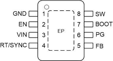
Figure 4-1 shows the LMR38010-Q1 and LMR38020-Q1 pin diagram. For a detailed description of the device pins please refer to the Pin Configuration and Functions section in the LMR38010-Q1 and LMR38020-Q1 data sheet.
 Figure 4-1 Pin Diagram
Following are the assumptions of use and the device configuration assumed for the pin FMA in this section:
- Application circuit, as per the LMR38020-Q1 SIMPLE SWITCHER® 4.2-V to 80-V, 2-A Synchronous Buck Converter Data Sheet
| Pin Name | Pin No | Description of Potential Failure Effect(s) | Failure Effect Class |
|---|---|---|---|
| GND | 1 | Normal operation | D |
| EN | 2 | VOUT = 0 V | B |
| VIN | 3 | VOUT = 0 V | B |
| RT/SYNC | 4 | Switching frequency >> 3 MHz | C |
| FB | 5 | VOUT >> than programmed output voltage | B |
| PG | 6 | No power-good function | B |
| BOOT | 7 | VOUT = 0 V | B |
| SW | 8 | Damage to HS FET | A |
| Pin Name | Pin No | Description of Potential Failure Effect(s) | Failure Effect Class |
|---|---|---|---|
| GND | 1 | VOUT can be abnormal due to switching noise on analog circuits. | B |
| EN | 2 | Device can shut off. | B |
| VIN | 3 | Device can shut off. | B |
| RT/SYNC | 4 | Switching frequency around a few10 Hz | B |
| FB | 5 | VOUT >> than programmed output voltage | B |
| PG | 6 | No power-good function | B |
| BST | 7 | VOUT = 0 V | B |
| SW | 8 | VOUT = 0 V | B |
| Pin Name 1 | Pin Name 2 | Description of Potential Failure Effect(s) | Failure Effect Class |
|---|---|---|---|
| GND |
EN |
VOUT = 0 V | B |
|
EN |
VIN |
Normal VOUT operation | B |
| VIN | RT/SYNC(1) | RT/SYNC Pin ESD damage if VIN > 5.5 V | B |
| FB | PG | VOUT less than programmed output voltage |
B |
| PG | BOOT | PGOOD pin ESD damage if BOOT pin voltage >20 V | A |
| BOOT | SW | VOUT = 0 V | B |
| Pin Name | Pin No | Description of Potential Failure Effect(s) | Failure Effect Class |
|---|---|---|---|
| GND | 1 | VOUT = 0 V. Damage to other pins referred to GND. | A |
| EN | 2 | Device enabled | D |
| VIN | 3 | Normal mode | D |
| RT/SYNC | 4 | RT/SYNC pin ESD damage if VIN > 5.5 V | B |
| FB | 5 | If VIN exceeds 5.5 V, damage will occur. VOUT = 0 V | A |
| PG | 6 | PGOOD pin ESD damage if VIN > 20 V | B |
| BOOT | 7 | VOUT = 0 V. CBOOT ESD clamp will run current to destruction. | A |
| SW | 8 | Damage to LS FET |
A |