SFFS303 October 2021 SN74LVC2G66-Q1
4 Pin Failure Mode Analysis (Pin FMA)
This section provides a failure mode analysis (FMA) for the pins of the SN74LVC2G66-Q1. The failure modes covered in this document include the typical pin-by-pin failure scenarios:
- Pin short-circuited to ground (see Table 4-2)
- Pin open-circuited (see Table 4-3)
- Pin short-circuited to an adjacent pin (see Table 4-4)
- Pin short-circuited to VCC (see Table 4-5)
Table 4-2 through Table 4-5 also indicate how these pin conditions can affect the device as per the failure effects classification in Table 4-1.
Table 4-1 TI Classification of Failure Effects
| Class | Failure Effects |
|---|---|
| A | Potential device damage that affects functionality. |
| B | No device damage, but loss of functionality. |
| C | No device damage, but performance degradation. |
| D | No device damage, no impact to functionality or performance. |
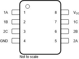
Figure 4-1 shows the SN74LVC2G66-Q1 pin diagram. For a detailed description of the device pins, see the Pin Configuration and Functions section in the SN74LVC2G66-Q1 data sheet.
 Figure 4-1 Pin Diagram
Table 4-2 Pin FMA for Device Pins Short-Circuited to
Ground
| Pin Name | Pin No. | Description of Potential Failure Effect(s) | Failure Effect Class |
|---|---|---|---|
| 1A | 1 | Corruption of analog signal on 1A. If there is no limiting resistor in the switch path device damage is possible. | A |
| 1B | 2 | Corruption of analog signal on 1B. If there is no limiting resistor in the switch path device damage is possible. | A |
| 2C | 3 | 2C stuck low. Cannot control switch states. | B |
| GND | 4 | No effect, normal operation. | D |
| 2A | 5 | Corruption of analog signal on 2A. If there is no limiting resistor in the switch path device damage is possible. | A |
| 2B | 6 | Corruption of analog signal on 2B. If there is no limiting resistor in the switch path device damage is possible. | A |
| 1C | 7 | 1C stuck low. Cannot control switch states. | B |
| VCC | 8 | Device unpowered. Device not functional. Observe that the absolute maximum ratings for all pins of the device are met, otherwise device damage is possible. | A |
Table 4-3 Pin FMA for Device Pins
Open-Circuited
| Pin Name | Pin No. | Description of Potential Failure Effect(s) | Failure Effect Class |
|---|---|---|---|
| 1A | 1 | Corruption of analog signal on 1A. | B |
| 1B | 2 | Corruption of analog signal on 1B. | B |
| 2C | 3 | Loss of control of IN pin. Switch in undefined state. | B |
| GND | 4 | Device unpowered. Device not functional. Observe that the absolute maximum ratings for all pins of the device are met, otherwise device damage is possible. | A |
| 2A | 5 | Corruption of analog signal on 2A. | B |
| 2B | 6 | Corruption of analog signal on 2B. | B |
| 1C | 7 | Loss of control of IN pin. Switch in undefined state. | B |
| VCC | 8 | Device unpowered. Device not functional. Observe that the absolute maximum ratings for all pins of the device are met, otherwise device damage is possible. | A |
Table 4-4 Pin FMA for Device Pins Short-Circuited to
Adjacent Pin
| Pin Name | Pin No. | Shorted to | Description of Potential Failure Effect(s) | Failure Effect Class |
|---|---|---|---|---|
| 1A | 1 | 1B | Corruption of analog signal on 1A. | B |
| 1B | 2 | 2C | Corruption of analog signal on 1B. | B |
| 2C | 3 | GND | 2C stuck to GND. Cannot control switch states. | B |
| GND | 4 | 2A | Not considered, Corner pin. | D |
| 2A | 5 | 2B | Corruption of analog signal on 2A. | B |
| 2B | 6 | 1C | Corruption of analog signal on 2B. | B |
| 1C | 7 | VCC | 1C stuck to VCC. Cannot control switch states. | B |
| VCC | 8 | 1A | Not considered, Corner pin. | D |
Table 4-5 Pin FMA for Device Pins Short-Circuited to
VCC
| Pin Name | Pin No. | Description of Potential Failure Effect(s) | Failure Effect Class |
|---|---|---|---|
| 1A | 1 | Corruption of analog signal on 1A. If there is no limiting resistor in the switch path device damage is possible. | A |
| 1B | 2 | Corruption of analog signal on 1B. If there is no limiting resistor in the switch path device damage is possible. | A |
| 2C | 3 | 2C stuck to VCC. Cannot control switch states. | B |
| GND | 4 | Device unpowered. Device not functional. Observe that the absolute maximum ratings for all pins of the device are met, otherwise device damage is possible. | A |
| 2A | 5 | Corruption of analog signal on 2A. If there is no limiting resistor in the switch path device damage is possible. | A |
| 2B | 6 | Corruption of analog signal on 2B. If there is no limiting resistor in the switch path device damage is possible. | A |
| 1C | 7 | 1C stuck to VCC. Cannot control switch states. | B |
| VCC | 8 | No effect, normal operation | D |