SFFS315 September 2022 TPS7B86-Q1
4.3 HSOIC Package B Version
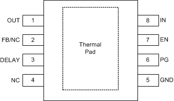
Figure 4-3 shows the TPS7B86-Q1 pin diagram for the HSOIC package B version with PG. For a detailed description of the device pins, see the Pin Configuration and Functions section in the TPS7B86-Q1 data sheet.
 Figure 4-3 Pin Diagram
 (HSOIC Package B Version With PG)
| Pin Name | Pin No. | Description of Potential Failure Effects | Failure Effect Class |
|---|---|---|---|
| OUT | 1 | Regulation is not possible, the device operates at current limit. The device can cycle in and out of thermal shutdown. | B |
| FB/NC | 2 |
(Fixed output.) No effect. Normal operation. (Adjustable output.) Output voltage is input voltage minus dropout voltage because the error amplifier drives the pass transistor gate to the rail. |
B/D |
| DELAY | 3 | Ground current is permanently increased. | C |
| NC | 4 | No effect. Normal operation. | D |
| GND | 5 | No effect. Normal operation. | D |
| PG | 6 | Power-good never asserts when the output voltage is at target, thus potentially effecting power sequencing. | B |
| EN | 7 | The device is disabled, resulting in no output voltage. | B |
| IN | 8 | Power is not supplied to the device. System performance depends on upstream current limiting. | B |
| Pin Name | Pin No. | Description of Potential Failure Effects | Failure Effect Class |
|---|---|---|---|
| OUT | 1 | The device output is disconnected from the load. | B |
| FB/NC | 2 |
(Fixed output.) No effect. Normal operation. (Adjustable output.) The error amplifier input is not connected. The output voltage is indeterminate. |
B/D |
| DELAY | 3 | The power-good delay is set to the minimum delay time t(DLY_FIX). | C |
| NC | 4 | No effect. Normal operation. | D |
| GND | 5 | There is no current loop for the supply voltage. The device is not operational and does not regulate. | B |
| PG | 6 | The power-good signal is not accessible. Power sequencing can be effected. | B |
| EN | 7 | The enable circuit is in an unknown state. The device can be enabled or disabled. | B |
| IN | 8 | Power is not supplied to the device, resulting in no output voltage. | B |
| Pin Name | Pin No. | Shorted to | Description of Potential Failure Effects | Failure Effect Class |
|---|---|---|---|---|
| OUT | 1 | FB/NC (pin 2) |
(Fixed output.) No effect. Normal operation. (Adjustable output.) Output voltage is equal to internal reference voltage. |
B/D |
| FB/NC | 2 | DELAY (pin 3) |
(Fixed output.) No effect. Normal operation. (Adjustable output.) PG can possibly never assert and the output voltage can thus be inaccurate. |
B/D |
| DELAY | 3 | NC (pin 4) | No effect. Normal operation. | D |
| GND | 5 | PG (pin 6) | Power-good cannot assert. Power sequencing can be affected. | B |
| PG | 6 | EN (pin 7) | Power-good functionality cannot operate correctly. PG can be damaged if the absolute maximum rating (20 V) is violated. | B/A |
| EN | 7 | IN (pin 8) | The device is always enabled when the input is powered. | B |
| Pin Name | Pin No. | Description of Potential Failure Effects | Failure Effect Class |
|---|---|---|---|
| OUT | 1 | Damage is possible if the absolute maximum rating is exceeded (20 V max). Reverse current can destroy the device. | A |
| FB/NC | 2 |
(Fixed output.) No effect. Normal operation. (Adjustable output.) The error amplifier input can be damaged. The output is not at the target voltage. |
A/D |
| DELAY | 3 | PG can incorrectly assert when the output voltage is not at target. The pin absolute maximum rating (6 V max) can be exceeded and the pin can be damaged. | B/A |
| NC | 4 | No effect. Normal operation. | D |
| GND | 5 | Power is not supplied to the device. System performance depends on upstream current limiting. | B |
| PG | 6 | Power-good functionality cannot operate correctly. PG can be damaged if the absolute maximum rating (20 V) is violated. | B/A |
| EN | 7 | The device is always enabled when the input is powered. | B |
| IN | 8 | No effect. Normal operation. | D |