SFFS379A September 2022 – March 2023 TLV766-Q1
1 Overview
This document contains information for the TLV766-Q1 (WSON package) to aid in a functional safety system design. Information provided are:
- Functional safety failure in time (FIT) rates of the semiconductor component estimated by the application of industry reliability standards
- Component failure modes and their distribution (FMD) based on the primary function of the device
- Pin failure mode analysis (pin FMA)
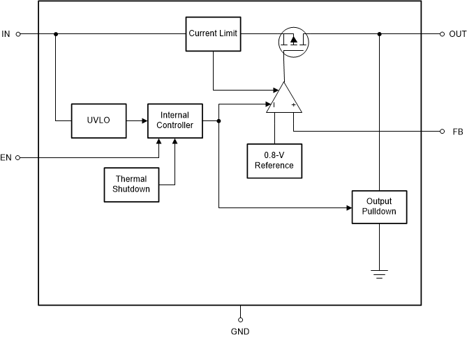
#GUID-E488EBD4-511E-41B0-B770-91A9719CA4DD shows the adjustable output device functional block diagram for reference.
 Figure 1-1 TLV766-Q1 Adjustable Output
Functional Block Diagram
Figure 1-1 TLV766-Q1 Adjustable Output
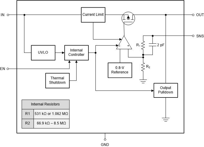
Functional Block Diagram#FIG_R43_RBX_KSB shows the fixed output device functional block diagram for reference.
 Figure 1-2 TLV766-Q1 Fixed Output
Functional Block Diagram
Figure 1-2 TLV766-Q1 Fixed Output
Functional Block DiagramThe TLV766-Q1 was developed using a quality-managed development process, but was not developed in accordance with the IEC 61508 or ISO 26262 standards.