SFFS496 June 2022 LMG1025-Q1
4 Pin Failure Mode Analysis (Pin FMA)
This section provides a failure mode analysis (FMA) for the pins of the LMG1025-Q1. The failure modes covered in this document include the typical pin-by-pin failure scenarios:
- Pin short-circuited to ground (see Table 4-2)
- Pin open-circuited (see Table 4-3)
- Pin short-circuited to an adjacent pin (see Table 4-4)
- Pin short-circuited to supply (see Table 4-5)
Table 4-2 through Table 4-5 also indicate how these pin conditions can affect the device as per the failure effects classification in Table 4-1.
| Class | Failure Effects |
|---|---|
| A | Potential device damage that affects functionality. |
| B | No device damage, but loss of functionality. |
| C | No device damage, but performance degradation. |
| D | No device damage, no impact to functionality or performance. |
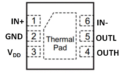
Figure 4-1 shows the LMG1025-Q1 pin diagram. For a detailed description of the device pins, see the Pin Configuration and Functions section in the LMG1025-Q1 data sheet.
 Figure 4-1 Pin Diagram
Following are the assumptions of use and the device configuration assumed for the pin FMA in this section:
- Adjacent short pin#1 to #6 and pin#3 to #4 are not considered.
- Short to supply is to VDD is considered.
| Pin Name | Pin No. | Description of Potential Failure Effect(s) | Failure Effect Class |
|---|---|---|---|
| IN+ | 1 | OUTH/L stuck low. | B |
| GND | 2 | No effect. | D |
| VDD | 3 | No power is applied to the device. | D |
| OUTH | 4 | OUTH/L stuck low. Possible damage to OUTH driver. | A |
| OUTL | 5 | OUTH/L stuck low. Possible damage to OUTH driver. | A |
| IN- | 6 | OUTH/L follows IN+ command. | B |
| Pin Name | Pin No. | Description of Potential Failure Effect(s) | Failure Effect Class |
|---|---|---|---|
| IN+ | 1 | OUTH/L stuck low. | B |
| GND | 2 | No power is applied to device. OUH/L pulled up to VDD. | B |
| VDD | 3 | No power is applied to device. | D |
| OUTH | 4 | OUTH is disconnected from the power stage gate. | D |
| OUTL | 5 | OUTL is disconnected from the power stage gate. | D |
| IN- | 6 | OUTH/L stuck low. IN- is pulled up. | B |
| Pin Name | Pin No. | Shorted to | Description of Potential Failure Effect(s) | Failure Effect Class |
|---|---|---|---|---|
| IN+ | 1 | GND | OUTH/L stuck low. | B |
| GND | 2 | VDD | No power is applied to device. | D |
| OUTH | 4 | OUTL | OUTH/L unknown. Possible damage to OUTH/L driver | A |
| OUTL | 5 | IN- | OUTH/L unknown. Possible damage to IN- I/O and OUTL driver. | A |
| Pin Name | Pin No. | Description of Potential Failure Effect(s) | Failure Effect Class |
|---|---|---|---|
| IN+ | 1 | OUTH/L stuck high. | B |
| GND | 2 | No power is applied to device. | D |
| VDD | 3 | No effect. Short to same potential. | D |
| OUTH | 4 | OUTH/L stuck high. Possible damage to OUTL driver. | A |
| OUTL | 5 | OUTH/L stuck high. Possible damage to OUTL driver. | A |
| IN- | 6 | OUTH/L stuck low. | B |