SLAA462A May   2010  – April 2019


  1.   EM430F6137RF900 Reference Design Guide
    1.     Trademarks
    2. 1 Impedance Matching and Filter Design Principles
      1. 1.1 Filter and Balun Layout Best Practices
    3. 2 EM430F6137RF900 RF Front End
      1. 2.1 Changing the RF Front End For 315 MHz
      2. 2.2 Changing the RF Front End For 434 MHz
    4. 3 EM430F6137RF900 Schematic Tips and Tricks
      1. 3.1 Achieving Successful BSL Communication
      2. 3.2 Communicating in Spy-Bi-Wire (SBW) Mode
    5. 4 ETSI Compliance
      1. 4.1 Capacitors on TMS, TDI, and TDO Pins
    6. 5 References
  2.   Revision History

Communicating in Spy-Bi-Wire (SBW) Mode

There is a row of six consecutive 0.1-in spacing jumpers populated at the top-center of the board. The two left-most jumpers in this set of six should be moved to connect to pins one and two on the header instead of pins five and six to successfully debug in Spy-Bi-Wire mode (see Figure 7).
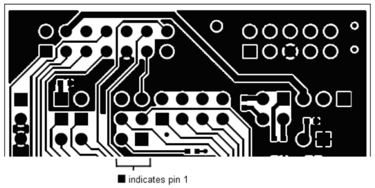
em430_front_sbw_comm_laa462.gifFigure 7. EM430F6137RF900 Front - SBW Communication