SLAA462A May 2010 – April 2019
1 Impedance Matching and Filter Design Principles
The CC430 MCUs have differential RF ports, RF_P and RF_N, that have an optimal impedance from the chip toward the antenna of Z = 86.5 + j43 Ω at 868 or 915 MHz and 116 + j41 Ω at 433 MHz.[6] The impedance of the selected antenna port is 50 Ω. Therefore, it is important to ensure proper impedance matching between the radio and the antenna through the use of a circuit network that translates a balanced signal from the CC430 to a 50-Ω unbalanced antenna load. This circuit is called a balun.
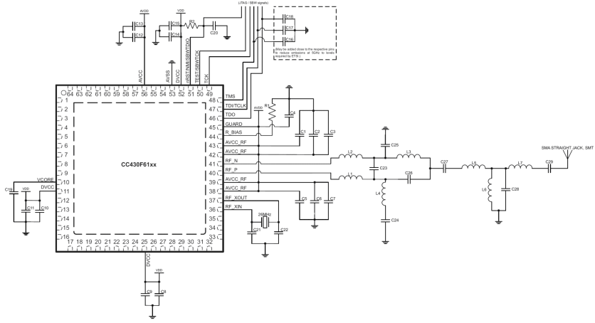
Figure 1 shows a typical application circuit for 868 or 915 MHz including the balun.
 Figure 1. Typical Balun Circuit for 868 or 915 MHz
 In transmit (TX) mode, the balun has two purposes:
- Provide optimum matching for the lowest possible current consumption and highest possible output power
- Fulfill regulatory harmonic and spurious emissions regulations
In receive (RX) mode, the balun has a single purpose:
- Provide optimum matching for the best possible sensitivity
The balun can be functionally divided into its different parts:
- Differential low-pass filter: L1, L2, C23
- Balun: C25, C26, L3, L4
- T-section band-pass filter: C27, C28, C29, L5, L6, L7
- DC block: C24
The recommended values of the balun components for different frequencies are in the EM430F6137RF900 target board files.
An ideal output signal from the CC430 in TX mode is a square wave signal at the RF_P and RF_N pins and a sine wave at the antenna port. To achieve this, the balun must successfully suppress the most prominent odd harmonics – the third and fifth – of the square wave. The lowest possible current consumption is achieved by having these odd harmonics reflected back towards the RF front-end with a high real part of the impedance. The easiest way to do this is through the use of the differential low-pass filter.
Following the low-pass filter is the balun that matches the impedance of the output to the 50-Ω node. The filter is designed to shift the output signal in phase by ±90° through the use of a low-pass and a high-pass filter. To achieve the best amplitude and phase balance in the balun, the layout trace from the single-ended port to each of the RF pins should be as equal in length and as symmetrical as possible. Any unbalance in the balun design causes high second and fourth harmonic levels, reduced output power at the single-ended side of the balun, higher transmit current consumption, and reduced sensitivity.
The filter that follows the balun is recommended to be T-type filter rather than a Pi-type to reduce the radiated emissions through shunt capacitors.
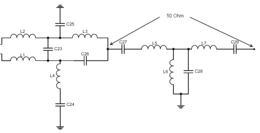
In the case of the EM430F6137RF900 target board, the filter is a band-pass filter and is dimensioned to have a 50-Ω impedance at both sides so it can easily be removed or redesigned to fulfill any special requirements (see Figure 2).
 Figure 2. 50-Ω Points in the Balun