SLAA705A July 2016 – November 2019 MSP430FR2310 , MSP430FR2311
2.1 Configuration of SAC_OA
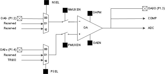
Figure 1 shows the block diagram of SAC_OA. The black squares are the control bits in the SAC0OA register. In addition to an external pin, the output of the SAC_OA is internally connected to inputs of the compare (eCOMP) and analog-to-digital converter (ADC) modules for further processing. The internal connections save pins so that signal is not routed out and then back into the device, which also can be advantageous in respect to noise. The control registers of the eCOMP and ADC modules must be configured to use this signal as input.
 Figure 1. SAC_OA Block Diagram
 To enable SAC_OA as a general-purpose operational amplifier, the OAEN, PMUXEN, and NMUXEN bits must be set in the SAC0OA register. Configure the OAPM bit to select high-speed or low-speed mode according to the application requirements. The high-speed mode enables faster slew rate at the cost of higher power consumption. The PSEL bits can be configured to connect the positive input to the external pin or TIA output.
Figure 2 shows the definition of the control register SAC0OA. For example, a value of 0x0588 must be written to the SAC0OA register to set up SAC_OA inputs to external pins and set SAC_OA in low-power low-speed mode.
| 15 | 14 | 13 | 12 | 11 | 10 | 9 | 8 |
| Reserved | SACEN | OAPM | OAEN | ||||
| r0 | r0 | r0 | r0 | r0 | rw-(0) | rw-(0) | rw-(0) |
| 7 | 6 | 5 | 4 | 3 | 2 | 1 | 0 |
| NMUXEN | Reserved | NSEL | PMUXEN | Reserved | PSEL | ||
| rw-(0) | r0 | rw-(0) | rw-(0) | rw-(0) | r0 | rw-(0) | rw-(0) |
The I/O pins on MSP430FR2311 are multiplexed with multiple module functions. The GPIO port control registers P1SEL0 and P1SEL1 must be configured to enable the SAC_OA function on the external pins. Figure 3 and Figure 4 show the definition of the P1SEL0 and P1SEL1 registers, respectively. Bits 2, 3, and 4 must be set in both the P1SEL0 and P1SEL1 registers to enable operational amplifier function on the external I/O pins.
| 7 | 6 | 5 | 4 | 3 | 2 | 1 | 0 |
| P1SEL0 | |||||||
| rw-0 | rw-0 | rw-0 | rw-0 | rw-0 | rw-0 | rw-0 | rw-0 |
| 7 | 6 | 5 | 4 | 3 | 2 | 1 | 0 |
| P1SEL1 | |||||||
| rw-0 | rw-0 | rw-0 | rw-0 | rw-0 | rw-0 | rw-0 | rw-0 |
As an example, use the code sequence in Example 1 to enable SAC_OA in low-speed mode with MSPWare driverlib APIs. In this example, all SAC_OA pins are routed to external I/O pins.