SLAA917A November 2019 – March 2020 MSP430FR2310 , MSP430FR2311 , MSP430FR2353 , MSP430FR2355
Design Goals
| Input | Output | Supply | ||||
|---|---|---|---|---|---|---|
| IiMin | IiMax | VoMin | VoMax | Vcc | Vref | |
| –1 A | 1 A | 100 mV | 3.2 V | 3.3 V | 1.65 V | |
Design Description
Some MSP430™ microcontrollers (MCUs) contain configurable integrated signal chain elements such as op-amps, DACs, and programmable gain stages. These elements make up a peripheral called the Smart Analog Combo (SAC). For information on the different types of SACs and how to leverage their configurable analog signal chain capabilities, visit MSP430 MCUs Smart Analog Combo Training. To get started with your design, download the Low-side Bidirectional Current Sensing Design Files.
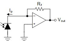
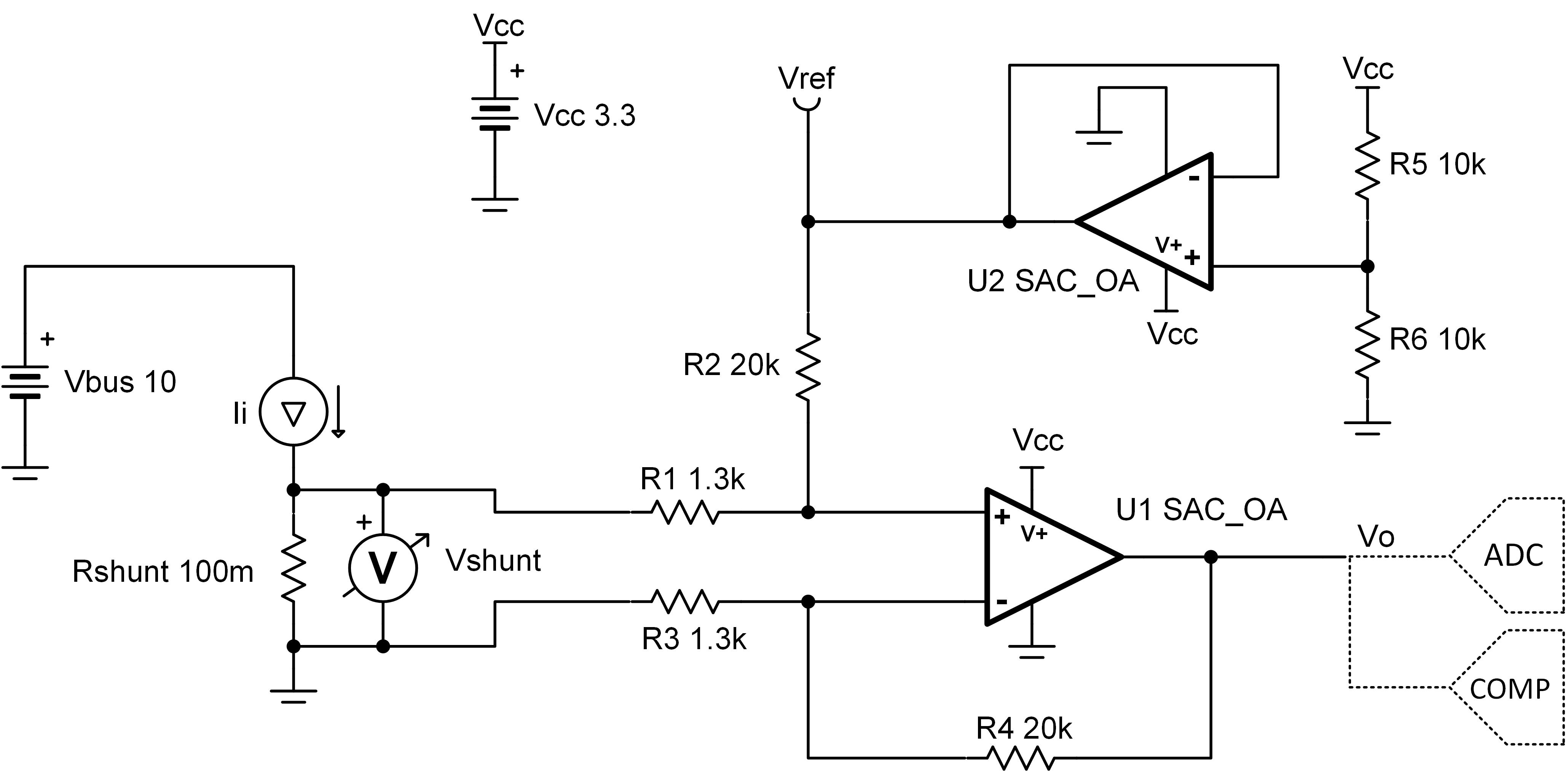
This single-supply low-side, bidirectional current sensing solution can accurately detect load currents from –1 A to 1 A. The linear range of the output is from 100 mV to 3.2 V. Low-side current sensing keeps the common-mode voltage near ground, and is thus most useful in applications with large bus voltages. This design leverages two of the four integrated op-amp blocks (SACs) in the MSP430FR2355 MCU. One SAC_L3 peripheral is configured as a general purpose op-amp to amplify the voltage across the shunt resistor, while the other is configured as a buffer to provide the bias voltage (Vref). The latter SAC_L3 block can also be configured in DAC buffer mode to provide Vref, replacing the external voltage divider circuit. The output of the circuit can be internally or externally connected to other integrated peripherals in the MSP430FR2355 MCU. For example, the analog-to-digital converter (ADC) window comparator can sample this output periodically (with no CPU intervention) and trigger an interrupt when the signal crosses a threshold.
Design Notes
- To minimize errors, set R3 = R1 and R4 = R2.
- Use precision resistors for higher accuracy.
- Set output range based on linear output swing (see Aol specification).
- Low-side sensing should not be used in applications where the system load cannot withstand small ground disturbances or in applications that need to detect load shorts.
- In the schematic above, the first SAC_L3 peripheral in the MSP430FR2355 MCU (U1) is configured in general purpose mode. The second SAC_L3 peripheral (U2) is also configured in general purpose mode, but with an external voltage divider.
- It is recommended to use the DAC buffer configuration for U2 (as seen in the code examples in the Low-side Bidirectional Current Sensing Design Files) to provide Vref instead of using the external voltage divider circuit.
- This solution can also be implemented using the MSP430FR2311 device by using the internal transimpedance amplifer for U1, and the SAC_L1 op-amp for U2.
- The Low-side Bidirectional Current Sensing Design Files include code examples showing how to properly initialize the SAC peripherals.
Design Steps
- Determine the transfer equation given R4 = R2 and R1 = R3.
- Determine the maximum shunt resistance.
- Set reference voltage.
- Because the input current range is symmetric, the reference should be set to mid supply. Therefore, make R5 and R6 equal.
- Set the difference amplifier gain based on the op amp output swing. The op amp output can swing from 100 mV to 3.2 V, given a 3.3-V supply.
Design Simulations
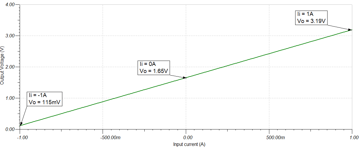
DC Simulation Results
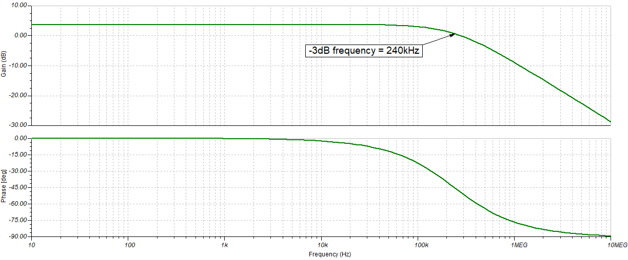
Closed Loop AC Simulation Results
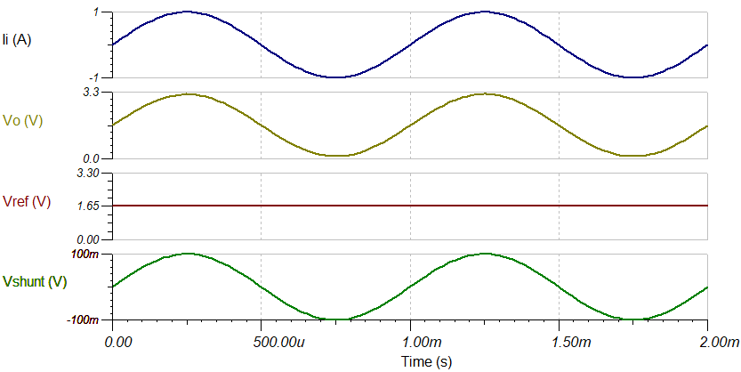
Transient Simulation Results
Target Applications
Servo Drive Funtional Safety Module
Battery Pack: Cordless Power Tool
Battery Pack: E-Bike/E-Scooter/Light Electric Vehicle (LEV)
Design References
- MSP430 Low-side Bidirectional Current Sensing Circuit Code Examples and SPICE Simulation File
- Analog Engineer's Circuit Cookbooks
- MSP430FR2311 TINA-TI Spice Model
- MSP430 MCUs Smart Analog Combo Training
Design Featured Op Amp
| MSP430FRxx Smart Analog Combo | ||
|---|---|---|
| MSP430FR2311 SAC_L1 | MSP430FR2355 SAC_L3 | |
| Vcc | 2.0 V to 3.6 V | |
| VCM | -0.1 V to VCC + 0.1 V | |
| Vout | Rail-to-rail | |
| Vos | ±5 mV | |
| AOL | 100 dB | |
| Iq | 350 µA (high-speed mode) | |
| 120 µA (low-power mode) | ||
| Ib | 50 pA | |
| UGBW | 4 MHz (high-speed mode) | 2.8 MHz (high-speed mode) |
| 1.4 MHz (low-power mode) | 1 MHz (low-power mode) | |
| SR | 3 V/µs (high-speed mode) | |
| 1 V/µs (low-power mode) | ||
| Number of channels | 1 | 4 |
| http://www.ti.com/product/MSP430FR2311 | ||
| http://www.ti.com/product/MSP430FR2355 | ||
Design Alternate Op Amp
| MSP430FR2311 Transimpedance Amplifier | |
|---|---|
| Vcc | 2.0 V to 3.6 V |
| VCM | -0.1 V to VCC/2 V |
| Vout | Rail-to-rail |
| Vos | ±5 mV |
| AOL | 100 dB |
| Iq | 350 µA (high-speed mode) |
| 120 µA (low-power mode) | |
| Ib | 5 pA (TSSOP-16 with OA-dedicated pin input) |
| 50 pA (TSSOP-20 and VQFN-16) | |
| UGBW | 5 MHz (high-speed mode) |
| 1.8 MHz (low-power mode) | |
| SR | 4 V/µs (high-speed mode) |
| 1 V/µs (low-power mode) | |
| Number of channels | 1 |
| http://www.ti.com/product/MSP430FR2311 | |
Related MSP430 Circuits