SLAA946 April 2021 AFE10004
6 Fast Output Switching
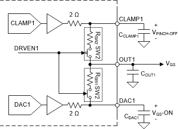
The AFE10004 uses two separate DAC channels to create the two critical bias voltages for the FET: the temperature compensated VGS-on voltage and the programmable, yet static, VGS pinch-off voltage. These are the DAC output and the CLAMP output, respectively. The gate of the FET is connected to a common node (OUT) that can be connected to either of the outputs through low RON switches. The outputs use external capacitors to quickly charge the common node to the desired voltage, rather than be limited to the current output and slew-rate of precision DACs, to switch the output voltage directly. The fast switching between the two voltages allows the PA to be turned on and off quickly, enabling burst transmission of the RF signal while reducing total power consumption.
 Figure 6-1 AFE10004 Output Switches