SLAAE45 September 2021 TMUXHS4412
3 Layout Examples
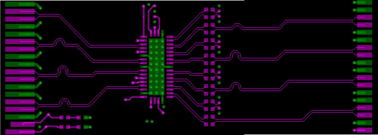
Figure 3-1 shows a TMUXHS4412 layout example.
 Figure 3-1 TMUXHS4412 Layout Example
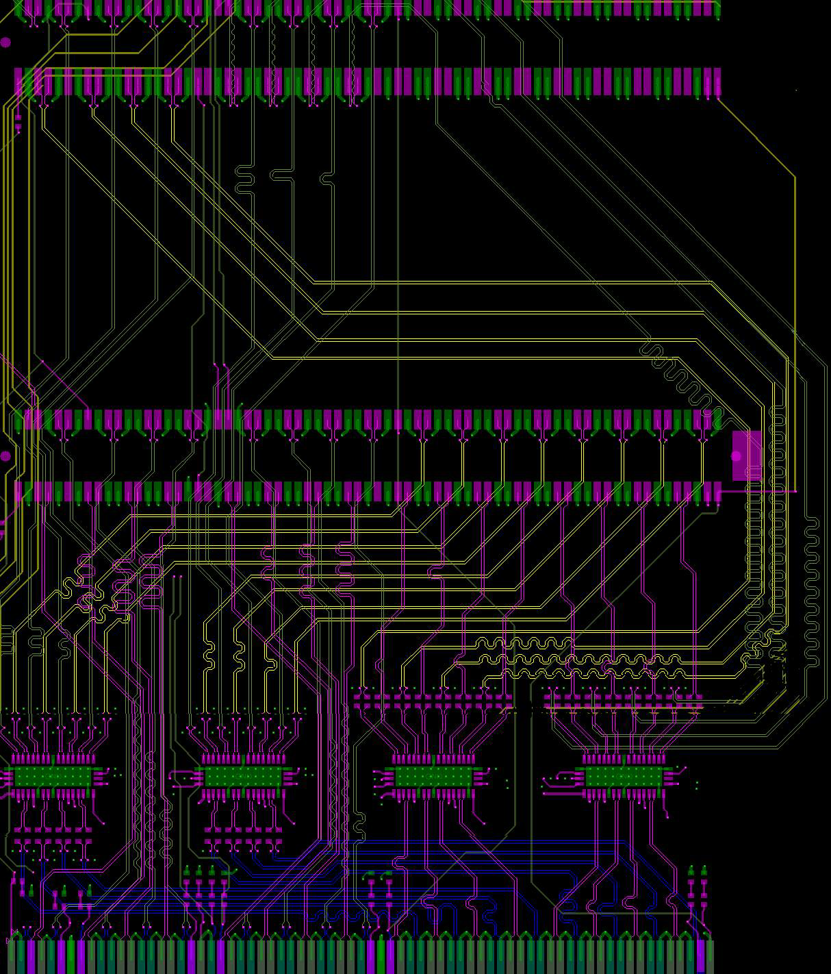
Figure 3-2 shows a layout illustration where four TMUXHS4412 are used to switch eight PCIe® lanes between two PCIe® connectors.
 Figure 3-2 Layout Example for PCIe® Lane MUXing Application